Revolutionary Steps in Nanotechnology and Smartphones
Nanotechnology is engineering, science, and technology conducted at the nanoscale.1 nanometer is a meter’s 10-9 or a meter’s billionth. Researchers want to make the materials at the nanoscale so they can have greater chemical reactivity, increased control of the light spectrum, lighter weight, and higher strength as compared to their larger-scale counterparts.
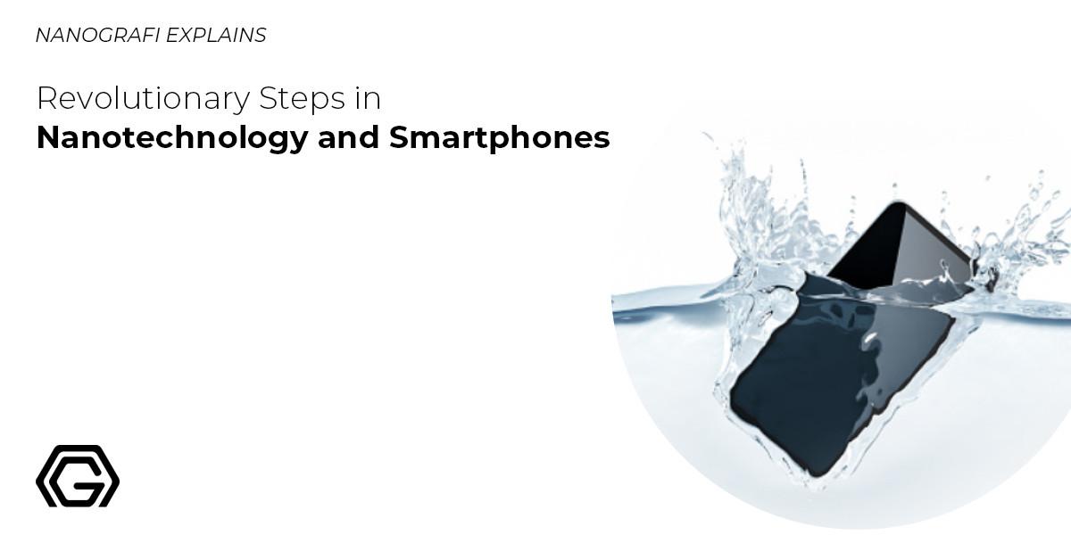
Now, nanotechnology can also be used to waterproof smartphones. In Asia, shops with special machines will take your smartphone and make them go through a cleaning process of 20 minutes and the application of nanocoating.
Introduction
Nanotechnology is technology, engineering, and science conducted at the nanoscale of around 1-100 nanometers. Application and studies of very small things are known as nanotechnology and nanoscience and they can be utilized across all of the other scientific fields like engineering, materials science, physics, biology, and chemistry.
An Overview of Nanotechnology and Waterproofing Technologies
A protective layer is also provided which makes the devices waterproof and stops the bacteria and dust from building up. The characteristic of nanotechnology to adapt to the user’s context is what makes it desirable to the consumer, along with being transformable and easy to use. Self-cleaning devices can be made on mobile devices by leveraging nanotechnology. Using nanotechnology can also allow us to make smaller and thinner batteries, so they can be quickly recharged, and way more charging cycles can be endured by them. Nanotechnology can make very high-speed radio-frequency amplifiers for wireless communications and cellular communications.
Concepts Behind Nanoscience and Nanotechnology
A talk known as 'There is plenty of room at the bottom' started the concepts and ideas behind nanotechnology and nanoscience at an American Physical Society meeting by physicist Richard Feynman on 29 December 1959 at the California Institute of Technology (CalTech), long before nanotechnology was utilized. A process was described by Feynman in which individual molecules and atoms could be manipulated by scientists. The term nanotechnology was coined by Professor Norio Taniguchi while he was exploring ultraprecision machining over a decade later. Individual atoms could be seen after the development of the scanning tunneling microscope which wasn't until 1981, which was started by modern nanotechnology.
Fundamental Concepts in Nanotechnology
Imagining how small nanotechnology is, gets difficult. 1 nanometer is a meter's 10-9 or a meter’s billionth. Some of the illustrative examples are mentioned here:
- In an inch, 25,400,000 nanometers are present.
- The thickness of a newspaper sheet is around 100,000 nanometers.
- In comparison, if a marble was a nanometer, then the Earth’s size would be one meter.
Control of Molecules and Atoms
Nanotechnology and nanoscience involve the capability of seeing and controlling individual molecules and atoms. Atoms have made up everything on the Earth, our bodies, our houses, buildings, clothes, and food. However, seeing something as small as an atom with the naked eye is impossible. Also, it is not possible to view with the microscopes that are utilized typically in science classes in high school. The early 1980s saw the invention of microscopes for being able to see things at the nanoscale. The nanotechnology age was born once the scientists had the right tools like the atomic force microscope (AFM), and the scanning tunneling microscope (STM).
Modern Nanotechnology
There has been the usage of nanoscale materials for centuries despite modern nanotechnology and nanoscience being quite new. Colors are created by the alternate-sized silver and gold particles in the medieval churches' stained glass windows, a decade ago. At that time, no artist knew the process that was utilized for creating these beautiful artworks which resulted in changes in the composition of the materials that they were using for work. A huge number of ways are being found by engineers and scientists for deliberately making the materials at the nanoscale so they can take benefit of their improved characteristics like greater chemical reactivity, increased control of light spectrum, lighter weight, and higher strength as compared to their larger-scale counterparts.
Usage of Modern Nanotechnology and Semiconductors in the Smartphones Industry
The University of Cambridge (UK) and Nokia Research Center (NRC), developed Nokia Morph, a joint nanotechnology concept that shows how the mobile devices of the future can be flexible and stretchable, thus enabling the user to convert their mobiles and devices into radically different shapes. All of this shows the significant role that nanotechnology can deliver; including self-cleaning surfaces, transparent electronics, and flexible materials.
Nanotechnology Offering Waterproofing Protection to Smartphones
There has been a continuous search by smartphone designers for ways to make the smartphone as attractive as possible, which includes the search for new technologies, for instance, the usage of nanotechnology for the waterproofing of smartphones. People somehow always accidentally get their phones wet which paves the way for the smartphone OEMs to utilize waterproofing nanotechnology as a major selling point for the latest devices.
Application of Coatings on a Walk-in Basis
Although the walk-in nanocoating practice is famous in Asian Countries only and is not that common in the world until now, there were reports of it in 2020 being used as a trend. One can go into the shop which has special machines and let their smartphones go through a cleaning process of 20 minutes and the application of the nanocoating. One shop provided a protective layer that not only just made the devices waterproof but also stopped the buildup of dust and bacteria.
Application of Coatings During the Manufacturing process
One method of the application of coating involves the utilization of a thin microscopic particle layer for filling in all of the surface's porous parts. Typically, these treatments occur before the end consumer receives the smartphone. According to statistics, this method can help the electronic bands in the reduction of the costs of repair when warranty claims or repair tickets are submitted by people for phones that are damaged by the water. One of the practical ways of protecting revenue is the integration of a nanotech coating process into production.
It is a surprise that each day almost 900,000 smartphones are damaged by liquids. Sony, Apple, and Samsung are some of the brands that provide waterproofing on smartphones. Water-resistant models are offered by other companies, offering a lesser degree of protection. The Doogee S96Pro Chinese phone for instance is dustproof and waterproof, plus made to meet some of the military specifications, like blast resistance.
Revolutionary Steps in Nanotechnology and Smartphones
Some of the revolutionary steps are showcased in technology by this device, which has the potential to result in a completely new spectrum of possibilities. Nanotechnology can enable way more intelligent devices and offer improved usability. Its characteristic of adapting to the user’s context is what makes it desirable to the consumer, along with its characteristic of being transformable and easy to use (wrapping it around the wrist for instance). It will provide our surroundings with a connectivity of a new kind, enabling us to link in ways through our mobile devices that no one ever thought of, and we will have a new type of service that is never seen before.
Some of the latest and new services are discussed below:
Flexible & Changing Design
Strong, transparent, stretchable, and flexible components and materials are enabled by nanotechnology. Thin elastic structures are reinforced by a three-dimensional mesh into which the fibril proteins are woven. Spider silk uses the same principle, as this elasticity allows the device to configure itself and change shapes for adapting ergonomically to the task at hand for being utilized as a traditional handset. More detailed information can be shown by an unfolded larger design, and it can also incorporate input devices like touchpads and keyboards. These flexible characteristics can be shared by even the integrated electronics, for the interconnects to the sensors. Recycling and production of devices can be made eco-friendly and easier by using biodegradable materials.
To learn more about the use of nanotechnology across different technologies,
you can read our blog post here.
Self-Cleaning
Self-cleaning devices can be made on mobile devices by leveraging nanotechnology, thus enhancing longevity, and lessening wear and corrosion. Fingerprints, dirt, and water are naturally repelled by the nanostructured surfaces like nanoflowers for using the effects that are seen in the natural systems too.
Advanced Power Sources
It is because of nanotechnology that the device’s surface will become energy’s natural source through a covering of the nanograss structures, which harvest the solar power. Batteries are allowed at the same time by the new high energy density storage materials for becoming thinner and smaller, they can be quickly recharged too, and way more charging cycles can be endured by them.
How Feasible is the Technology?
Morph concept shows the integrated electronics which are less expensive and have more features in a way smaller space, even as the enhancement of the usability and simplification of the interfaces. New services and applications will be unleashed by all of these new capabilities that will enable us the communication and interact in unprecedented ways.
Future of the Phone in the Market
Morph's elements are available in the market for their integration into handheld devices in 7 years, only at the high end though initially. Although, one-day nanotechnology may result in low-cost manufacturing solutions, and provide the possibility of integration of the complex functionality at a lower price.
Future of the Appearance of Mobile Phones
For NRC, nanotechnology is just one of the key future research areas, but it is a significant one as it will provide us the chance of designing the materials through the manipulation of the molecules and atoms at the nanometer level. Thus, it can be both revolutionary and evolutionary when implemented in mobile technology. In the next some years, new and innovative characteristics will be possessed by the phones that will be more unusual than the ones that are being utilized broadly today.
Usage of New Nanoscale Structure
Led by Professor Stephen Chou, an electrical engineering professor, the researchers used a new nanoscale structure for increasing the efficiency and brightness of the LEDs are 57% made up of organic materials (flexible carbon-based sheets). A method is also reported by the researchers which must use similar enhancements in the LEDs that are made of inorganic (silicon-based) materials and are most commonly utilized today.
Clarity of LED
LED displays picture clarity is also improved by 400% through this method more than conventional approaches. On August 19, an article was published online in the journal Advanced Functional Materials in which it was described by the researchers how they invented a method that is used for the manipulation of light on a scale that is smaller than a single wavelength. According to Chou, the rules of how we manipulate light can be changed by the new nanotechnology. This can be used for the production of devices with unimaginable performance.
Light-Emitting Diode
A LED is an electronic device emitting light when there is a movement of an electrical current between the two terminals. Several benefits are offered by the light-emitting diodes over fluorescent or incandescent lights. LEDs are way more compact, efficient, and with a longer lifetime comparatively, and all of these characteristics are considered significant in portable displays.
Current LEDs
There are design challenges in the current light-emitting diodes, the most important one is lessening the light's amount that is trapped inside the structure of the light-emitting diodes. Despite being famous for their efficiency, only an extremely small amount of light is produced inside a light-emitting diode escape. According to Chou, the same is the reason why the lighting inside a swimming pool looks dim when you see it from outside and that is because the light is trapped by the water. LED's solid structure is capable of trapping way more light as compared to the water of the pool.
Rudimentary LED
Only 2-4% of the generated light is emitted by a rudimentary LED. Not only the trapped light makes the light emitting diodes energy inefficient and dim, but the trapped light also is the reason for them being short-lived as the LED is heated by the trapped light, thus significantly lessening its lifespan. Chou said that light extraction is the holy grail in the manufacturing of LED today.
Additional Work on the Problems
This problem is being solved by the engineers. The light extraction of the LEDs can be increased by adding lenses, metal reflectors, or other structures. Light extraction for these conventional organic, high-end LEDs can be increased by these methods to about 38%. However, these light-extraction methods are the reason for the displays being capable of reflecting ambient light, thus reducing the contrast and making the image seem hazy.
Combating the Light’s Reflection
Now the engineers have added light-absorbing materials to the display for combating the ambient light's reflection. However, according to Chou, light is also absorbed from the LED by such materials, lessening its efficiency and brightness by half.
If you are interested in the uses of graphene in daily life,
you can read our blog post here.
The Solution
Chou's team presented the solution which is the production of a nanotechnology structure that is known as PlaCSH (plasmonic cavity with subwavelength hole array). According to researchers, the efficiency of light extraction can be increased by the PlaCSH to 60%, which is 57% more as compared to the conventional high-end organic light-emitting diodes. According to the reports of the researchers at the same time, the contrast was increased by 400 % by PlaCSH (clarity in ambient light). The heating problem due to the light that is trapped in the standard light-emitting diodes is relieved by the higher brightness.
Results
According to Chou, PlaCSH can obtain these results as its metallic nanometer-scale structures can manipulate light in such a way that non-metallic nanostructures and bulk material can’t.
Structure of Solar Cells
PlaCSH structure was first used by Chou on the solar cells, converting light into electricity. It was explained by him in a paper in 2012 how the PlaCSH application led to the absorption of as much as 96% of the light striking the surface of the solar cells and increased the efficiency of the cells by 175%. It was then realized that a device that can absorb light from the outside can be good at the radiation of light that is produced inside the device, providing an effective solution for both extractions of light and reduction of the light reflection.
Guiding the Light
PlaCSH can focus more light toward the viewer because it functions by guiding the light out of the light-emitting diode. The conventional brittle transparent electrode is also replaced by the system, making it way more flexible as compared to the most current displays. According to Chou, it is so ductile and flexible that one can weave it into cloth.
The Benefit of Cost
Cost is another advantage for the producers. In 1995, Chou invented a technology known as nanoimprint which made the PlaCSH organic light-emitting diodes, creating nanostructures in a fashion that is alike to the printing press generating newspapers. According to Chou, it is very simple and cheap.
Patent Applications
Patent applications have been filed by Princeton for both inorganic and organic light-emitting diodes by utilizing PlaCSH. Right now, experiments are being conducted by Chou and his team for demonstrating the PlaCSH in blue and red organic light-emitting diodes, other than the green light-emitting diodes that are being currently utilized in the experiments. The system in inorganic light-emitting diodes is also demonstrated by them.
Carbon Nanotube Applications in Smartphones Graphene Mobile Batteries
In 2014, it had been reported that CNT chips were made to be ready for being utilized commercially in 2020. Although it has been reported that there were still signs of struggle in figuring out the way to shrink the battery’s oxide without the battery leaking.
Carbon Nanotube Transistors
It is confirmed that theoretically, carbon nanotube transistors are way faster as compared to silicon transistors but recently, researchers were presented with the challenge of removing the impurities in them. Only two-thirds of the grown carbon nanotubes turn into the semiconducting variety that is required for transistors when the CNTs are grown. Arnold's lab could make conditions in which almost 99.9% of the tubes were semiconducting.
Rapid Enhancements
There have been rapid enhancements in carbon nanotube technology in the past few years, but there are still challenges regarding the utilization of the actual technology. Until now they have only tested the enhanced transistors on an inch-by-inch scale which is hardly enough for determining if they are capable of being utilized in a CPU that can take 100 transistors to function.
Immediate Impact
An immediate impact can be made by utilizing nanotechnology on a smaller scale. Nanotubes provide a good alternative to silicon for the future of wearable electronics because of their flexibility of the nanotubes. It also makes extremely high-speed radio-frequency amplifiers for wireless communications and cellular communications.
Substantial Progress
There has been a substantial improvement over the past decade in the production of flexible electronic devices like implantable biomedical devices, active radio frequency identification (RFID) tags, wearable electronics, and roll-up displays.The development of suitable stretchable and flexible energy storage devices is increasingly important as these devices go more close to their commercialization.
Lithium-Ion Battery Technology for Smartphones
Currently, the Lithium-ion battery technology has the most chance of obtaining the power and energy density that is needed for these applications, and that's why it is important to understand the mechanical stress impact because of the bending on the electrodes and the way to enhance their flexibility. There are several ways to increase their flexibility and robustness, for instance, embedding the active materials in plastic, paper, fabrics, or porous substrates, patterning or structuring the collector electrode, and decreasing the thickness of the battery electrode layers. The batteries are assembled from freestanding electrode films.
Conclusion
Nanotechnology can deliver significant functions; including self-cleaning surfaces, transparent electronics, and flexible materials. Now, one can also use nanotechnology for the waterproofing of smartphones. Nanotechnology can enable way more intelligent devices and offer improved usability. Nanotubes provide a good alternative to silicon for the future of wearable electronics.
References
2 Best Ways to Synthesis of Carbon Nanotubes - Nanografi Nano Technology. (n.d.). Retrieved April 19, 2024, from https://nanografi.com/blog/2-best-ways-to-synthesis-of-carbon-nanotubes/
14 Uses of Graphene In Daily Life - Nanografi - Nanografi Nano Technology. (n.d.). Retrieved April 19, 2024, from https://nanografi.com/blog/14-uses-of-graphene-in-daily-life-nanografi/
Anti-Corrosive Nanocoatings - Nanografi Nano Technology. (n.d.). Retrieved April 19, 2024, from https://nanografi.com/blog/anticorrosive-nanocoatings/
Application Areas of Nanotechnology in Display and Communication Technology - Nanografi Nano Technology. (n.d.). Retrieved April 19, 2024, from https://nanografi.com/blog/application-areas-of-nanotechnology-in-display-and-communication-technology/
Carbon Nanotubes Might Be The Key To Faster Phones. (n.d.). Retrieved April 19, 2024, from https://www.inverse.com/article/20664-carbon-nanotubes-cpu-phones-wisconsin
Commercial Value and Benefits of Carbon Nanotubes Transistors - Nanografi Nano Technology. (n.d.). Retrieved April 19, 2024, from https://nanografi.com/blog/commercial-value-and-benefits-of-carbon-nanotubes-transistors/
Facts about Aluminum (Al) Nanoparticles/Nanopowder - Nanografi Nano Technology. (n.d.). Retrieved April 19, 2024, from https://nanografi.com/blog/facts-about-aluminum-al-nanoparticlesnanopowder/
Following the Natures Lead: Lotus Effect Self-Cleaning - Nanografi Nano Technology. (n.d.). Retrieved April 19, 2024, from https://nanografi.com/blog/following-the-natures-lead-lotus-effect-selfcleaning/
Future of Solar Cells with Nanotechnology Solar Energy - Nanografi Nano Technology. (n.d.). Retrieved April 19, 2024, from https://nanografi.com/blog/future-of-solar-cells-with-nanotechnology-solar-energy/
Gallium Arsenide Wafers - Nanografi Blog - Nanografi Nano Technology. (n.d.). Retrieved April 19, 2024, from https://nanografi.com/blog/gallium-arsenide-wafers/
Gold (Au) Element’s Specifications - Nanografi Nano Technology. (n.d.). Retrieved April 19, 2024, from https://nanografi.com/blog/gold-au-elements-specifications/
Graphene and Carbon Nanotube Applications in Mobile Devices | Request PDF. (n.d.). Retrieved April 19, 2024, from https://www.researchgate.net/publication/253240051_Graphene_and_Carbon_Nanotube_Applications_in_Mobile_Devices
Graphite Sheet as Brilliant Thermal Interface Material - Nanografi Nano Technology. (n.d.). Retrieved April 19, 2024, from https://nanografi.com/blog/graphite-sheet-as-brilliant-thermal-interface-material/
History, Scope and Future of Nanotechnology - Nanografi Nano Technology. (n.d.). Retrieved April 19, 2024, from https://nanografi.com/blog/history-scope-and-future-of-nanotechnology/
Indium Tin Oxide and Its Applications On Mobile Device Screens - Nanografi Nano Technology. (n.d.). Retrieved April 19, 2024, from https://nanografi.com/blog/indium-tin-oxide-and-its-applications-on-mobile-device-screens/
Ink-Jet Printing of Graphene for Flexible Electronics - Nanografi Nano Technology. (n.d.). Retrieved April 19, 2024, from https://nanografi.com/blog/inkjet-printing-of-graphene-for-flexible-electronics/
Jessl, S., Beesley, D., Engelke, S., Valentine, C. J., Stallard, J. C., Fleck, N., Ahmad, S., Cole, M. T., & De Volder, M. (2018). Carbon nanotube conductive additives for improved electrical and mechanical properties of flexible battery electrodes. https://doi.org/10.1016/j.msea.2018.08.033
Lithium-Ion Batteries: How They Work, Where They Are Used, Advantages & Disadvantages - Nanografi Nano Technology. (n.d.). Retrieved April 19, 2024, from https://nanografi.com/blog/lithiumion-batteries-how-they-work-where-they-are-used-advantages-disadvantages/
Nanotechnology Applications in Daily Life - Nanografi Nano Technology. (n.d.). Retrieved April 19, 2024, from https://nanografi.com/blog/nanotechnology-applications-in-daily-life/
Nanotechnology leads to better, cheaper LEDs for phones and lighting. (n.d.). Retrieved April 19, 2024, from https://www.princeton.edu/news/2014/09/24/nanotechnology-leads-better-cheaper-leds-phones-and-lighting
Nokia Morph | Nanotechnology, the future of mobile phones | Mint. (n.d.). Retrieved April 19, 2024, from https://www.livemint.com/Leisure/26NyPbNv7MCT7P1lSOMFZI/Nokia-Morph--Nanotechnology-the-future-of-mobile-phones.html
Silver Element’s Specifications and Applications - Nanografi Nano Technology. (n.d.). Retrieved April 19, 2024, from https://nanografi.com/blog/silver-elements-specifications-and-applications/
Strategies for Improving Rechargeable Lithium-ion Batteries - Nanografi Nano Technology. (n.d.). Retrieved April 19, 2024, from https://nanografi.com/blog/strategies-for-improving-rechargeable-lithiumion-batteries/
The Internet of Things: The next growth engine for the semiconductor industry. (n.d.). Retrieved April 19, 2024, from www.pwc.com
Use of Graphene in Electronics - Nanografi Nano Technology. (n.d.-a). Retrieved April 19, 2024, from https://nanografi.com/blog/use-of-graphene-in-electronics/
Use of Graphene in Electronics - Nanografi Nano Technology. (n.d.-b). Retrieved April 19, 2024, from https://nanografi.com/blog/use-of-graphene-in-electronics/
Using Nanoimprinting with Applications in Optics - Nanografi Nano Technology. (n.d.). Retrieved April 19, 2024, from https://nanografi.com/blog/using-nanoimprinting-with-applications-in-optics/
Recent Posts
-
Reducing the Carbon Footprint of Nanomaterials
The production of nanomaterials is vital for numerous advanced applications, from healthcare to elec …26th Apr 2024 -
Nanocomposites in Food Packaging
The utilization of nanocomposites in food packaging represents a significant advancement in the fiel …19th Apr 2024 -
What is the Difference Between 7075 and 6061 Aluminum Alloy?
When comparing 7075 aluminum alloy to 6061 aluminum alloy, it's essential to understand their disti …5th Apr 2024


