
Using Nanoimprinting with Applications in Optics
Large area nanoimprinting lithography is classified among the most promising technologies of micron and nanoscale manufacturing for the purpose of large-area patterns mass production, complex 3D structures as well as high aspect ratio features and practically high throughput and high resolution at low cost.
This technology makes it possible for many commercial applications to make huge progress. In fact, achievements in the field of large-area nanoimprinting has come true in the past years with solutions to improve mass production of nanostructures over large areas in distinct substrates and surfaces. Furthermore, numerous industrial level applications and creative products that are basically based on large area nanoimprint lithography. Production of nanostructured materials over large areas and in bigger scales is considered crucial for them to be applied for commercial purposes in nanotechnology. Discover Nanografi's high-quality nanomaterials now, with experience in working and collaborating in the markets of over 100 countries worldwide.
Introduction
It has been demonstrated that large-area nanopatterning has huge potentials to enhance the functionality and performance of many devices and give rise to even more creative and innovative products including hard disk drivers, displays, anti-reflective glass, sub wave-length optical elements and flexible electronics. Solar cells for instance, show a higher photocurrent and higher power conversion efficiency when coated with anti-reflective nanostructures compared to those which exclude nanomaterials in their structure. Another example is sapphire lights with nanopatterns and photonic crystals that are known to be the most effective techniques to enhance the light output efficiency or internal and external quantum efficiency and beam shaping and LEDs. Nevertheless, it is really challenging to employ current patterning techniques in mass production specifically, nanopatterning in distinct non-flat or curved surfaces as well as flexible and fragile substrate 1.

Nanoimprinting Lithography
Nanoimprinting lithography (NIL) is considered to be a promising technique of nanopatterning basically employed to fabricate the large-area nanoscale patterns. In fact, the NIL is listed among the 10 most emerging technologies capable of affecting the nanotechnology. Is technology, it is expected to serves as a critical factor in commercialization of nanostructured materials. Particularly, a broad range of emerging large-area NIL processes including wafer scale soft UV-NIL process, roll-to-plate NIL, roll-to-roll NIL process provide practical solutions and reliable tools for mass production of nanostructures in the nanoscales with low cost and higher efficiencies and applications in laser level optical element, compound semiconductor optoelectronics nanophotonic devices and more specifically LED patterning using wafer nanoimprinting lithography and anti-reflective and coatings through roll-to-roll imprinting process 1.
Photopolymerization
Polymerization is a common production procedure employed in a variety of areas of electronics and industries. Particularly, it is technique employed to manufacture optical discs, optical waveguides, laser light pens and aspherical lenses. For instance, submicron pits are compressed and copied onto some special discs to produce optical disc masters. Based on this process, aspherical lenses with applications in compact discs with 50 nm accuracy are produced. These days in semiconductor industry, structures of 0.25-mm and even 0.18-mm are still fabricated taking the advantage of optical lithography but are limited because of their dimensions. It is possible to consider structures with even smaller sizes based on extreme UV lithography, beam projection lithography, electron beam projection lithography and x-ray. Technically, the replication process leads to the manufacturing of structures with dimensions below 100 nm. In this case, the image transfer system control is this only a UV light source at practically low cost and simple mechanism.

Figure 1. Different types structures of polymers by polymerization.
Nanopatterning
Currently, optical lithography is employed as the predominant lithography technology with applications in the semiconductor industry however, its survival closely depends on achievements in its integration with other techniques to get over the physical limits and that the cost of optical lithography devices is almost high. In fact, there are two main approaches of nanopatterning over a large area including bottom-up approach which involves the self-assembly or direct assembly and the top down approach like photolithography. Optical or photolithography was previously employed to manufacture printing plates prior to emergence of semiconductors and now it is the technology of manufacturing semiconductors of sizes of more than 2 macrons to as small as 32 nm in complementary metal-oxide semiconductors. The process of nanopatterning that is widely employed in current technology is getting more and more expensive and complicated as it is getting to even a smaller scales with the increasing demand by the industry. On the other hand the introduction of shrinking photon the growing application of resolution enhancement techniques and increasing optic numerical have contributed a lot to the growth of optical lithography. At the moment extreme ultraviolet lithography has promising results in semiconducting Industries and has been supported buy a lot of semiconductor industry companies from around the world which is basically due to the fact that this technology depends on an extended optical lithography technique at shorter wavelength to illuminating light 2.
Processes of Large Area Nanoimprinting Lithography
Up to this point, several large-area nanoimprinting lithography (NIL) processes have been suggested and developed with applications in science and industries. Depending on the types of molds, imprinting continuity and imprint contacts, the large-area the NIL technology is categorized into two fundamental classes as the full wafer nanoimprinting lithography and roller type nanoimprinting lithography. Roller-type NIL itself is classified into two other subclasses including roll-to-plate (R2P) NIL and roll-to-roll (R2R) NIL among which R2R NIL process is considered to have a promising future to be implemented as a full scale process mainly because of its large area patterning quality and high throughput capability with continues roller pressing process which is also employed in many industrial applications at the moment.
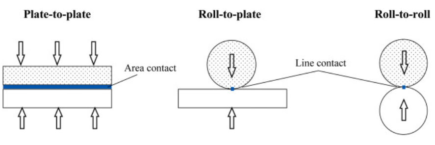
Figure 2. Three main contact types of NIL processes.
Full Wafer Nanoimprint Lithography (plate-to-plate type NIL, batch press type)
In full wafer NIL process, a flexible and flat mold or stamp is employed to compress into a substrate with rigid nature leading to a full field contact. A soft UV-NIL using a soft or flexible mold has been demonstrated to be a desirable technique to fabricate large area patterns in the nanometer-scale in order to design and pattern full wafer area with no high imprinting and the molding forces. The strength of this process are sequential imprinting, peel-off demolding and flexible mold. Another novel large area wafer is nanoimprinting methods based on substrate lithography which capable of bridging the gap between large areas of imprint and small rigid imprint stamp as best resolution with practically limited resolution. In fact, NIL is restricted by practicable reasons in imprint area mostly because of the waviness of substrates. The implementation of full wafer NIL requires the application of the composite mold and the sequential imprinting methods. Basically, the composite mold is made of to rubber layers designed on stained glass support. The in-plane stiffness of the stamp faces no pattern deformation over large areas, whereas out-of-plane flexibility allows conformal contact to underlying surface features.

Conclusion
Nanoimprinting lithography has moved from a novel and exciting research topic to emerge as a technology employed in the most advanced parts of modern-age industries in the past two decades. Large-area nanoimprinting lithography is considered as a cost effective and high-volume nanopatterning technique for large-area structure replication mostly in the nanometer-scale to fabricate complex 3D nanostructures and large-area patterns, non-planar surfaces and curved substrates. This technology has provided a promising solution and practical solution for mass production of nanostructures at low cost and higher efficiency for applications in anti-reflective coatings and films, solar cells, architectural glasses, LEDs, optical elements, micro-lenses, patterned media, wire grid polarizers and functional polymer devices.
To get more information, you can visit Blografi.
References
Adiloğlu, S. et al. We are IntechOpen , the world ’ s leading publisher of Open Access books Built by scientists , for scientists TOP 1 %. Intech i, 13 (2012).
Mohamed, K. Nanoimprint lithography for nanomanufacturing. Compr. Nanosci. Nanotechnol. 1–5, 357–386 (2019).
Polymer (matrix) structure - A236 - CKN Knowledge in Practice Centre. (n.d.). Retrieved January 26, 2024, from https://compositeskn.org/KPC/A236
Three main contact types of NIL processes. | Download Scientific Diagram. (n.d.). Retrieved January 26, 2024, from https://www.researchgate.net/figure/Three-main-contact-types-of-NIL-processes_fig3_263933703
Recent Posts
-

Nanocomposites in Food Packaging
The utilization of nanocomposites in food packaging represents a significant advancement in the fiel …19th Apr 2024 -

What is the Difference Between 7075 and 6061 Aluminum Alloy?
When comparing 7075 aluminum alloy to 6061 aluminum alloy, it's essential to understand their disti …5th Apr 2024 -

Iron-Air Batteries: The Ultimate Guide
Iron-air batteries represent a significant breakthrough in energy storage technology, offering a sus …29th Mar 2024