Reasons Why Graphene Oxide Is Leading the Graphene Industry, Its Properties, Applications, and Potentials
Graphene is one of the most remarkable and exciting materials to ever exist. It is an allotrope of carbon which in the form of a honeycomb, becomes a lattice that is throughout the industry known as graphene.
It is very much renowned as it exhibits properties that are highly remarkable and authentic for example exceptional surface area, good thermal conductivity, good density, etc. All these properties when combined make up a great product that is graphene and then further used for different purposes. Graphene has a lot of products but the most leading one is graphene oxide which due to its remarkability and efficacy has made its way in the industry as one of the best products. Graphene oxide has further its properties and applications which extinguish it from the rest of the materials that graphene produces. All these applications are a source of enhancing the credibility of graphene oxide as they are a part of the process which goes behind the flourishment of the product and along with it all the products that it is a part of. All the reasons due to which graphene oxide is proved as the leading product of the graphene industry are explained in this article.
Introduction
Being an exciting material, Graphene is used in numerous applications, for instance, for the transparent conductive electrodes as graphene has good electrical conductivity, good optical transmittance (∼ 97.7%), good thermal conductivity (∼ 5000 Wm − 1 K – 1), high Young’s modulus (∼ 1.0 TPa), high intrinsic mobility (200 000 cm 2 v − 1 s − 1), and a large theoretical specific surface area (2630 m 2 g − 1).
For 40 years, experimental studies are being conducted on graphene, and measurements of transport characteristics in the micro mechanically exfoliated layers, of the SiC-grown graphene, copper substrates-grown large-area graphene, and also different studies involving chemically modified graphene’s (CMG) usage in making new materials, resulted in an increase in the number of publications. There are unlimited possibilities given by the graphene for its carbon backbone’s functionalization or modification as it is robust and still a flexible membrane.
In CMG's synthesis on a ton scale, the huge potential is shown by the Graphene oxide (GO). Here, graphene's and CMG's (specifically graphene oxide) potential applications, physical characteristics, and production are discussed in detail. There are numerous reviews on graphene and its related materials now. The graphene oxide's chemistry, graphene's chemistry, and GO-derived exfoliated platelets chemistry reviews have also been noted. For a few layers (3 to 10 layers), bilayer, and monolayer graphene or graphene-based materials that are derived from graphene oxide, the applications will be discussed.
Why is Graphene Oxide Leading the Graphene Industry?
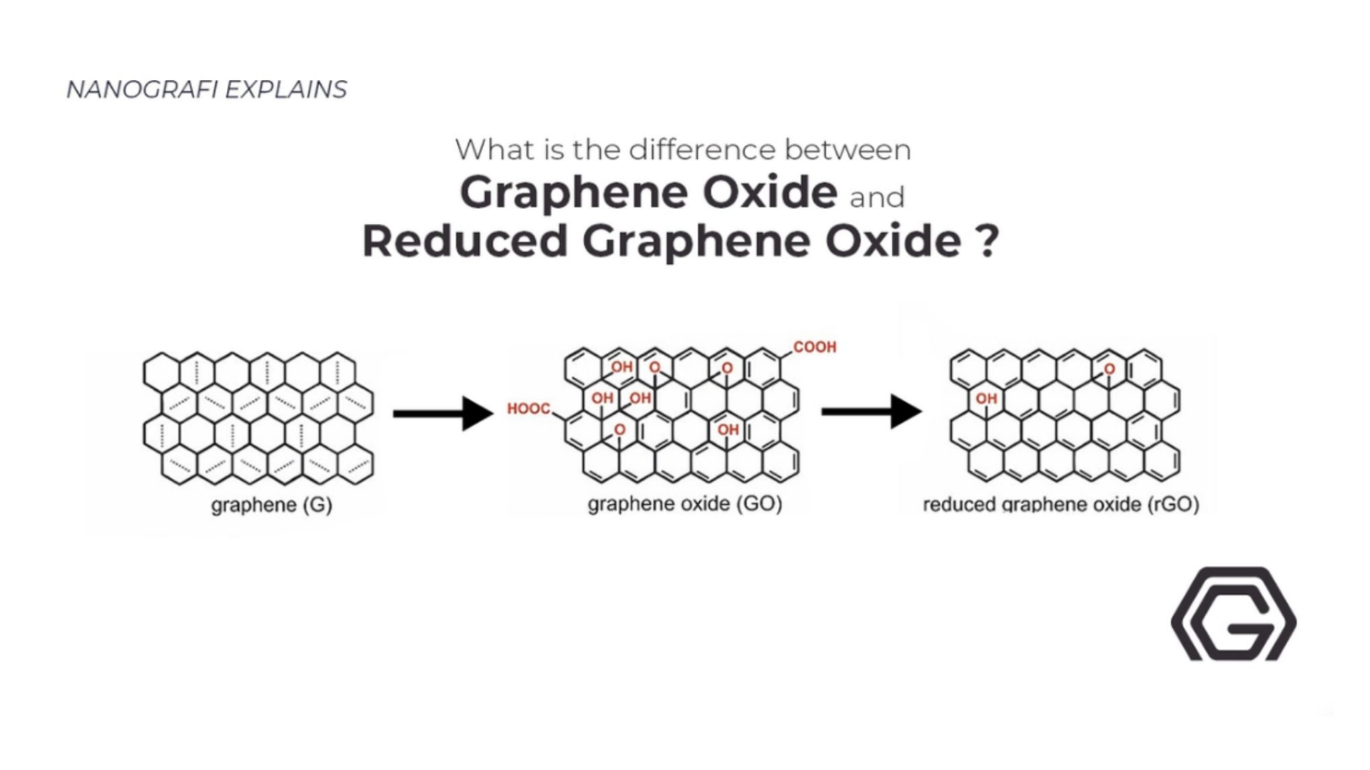
Graphene's oxidized form is Graphene oxide (GO). Already available and cheap, Graphite’s oxidation can form a single-atomic-layered material. Due to being dispersible in other solvents and water, the processing of graphene oxide is easy. In Graphene oxide’s lattice, oxygen is present, making it non-conductive but by proper chemical approaches, graphene oxide is capable of being reduced to graphene.
The reasons for which graphene oxide is leading the graphene industry lies in the properties and applications of graphene oxide, both of which are briefly explained below as they are potentially so strong that they make graphene oxide, the leading product of graphene.
Properties of Graphene Oxide
Morphology and Structure
Carbon atoms’ two equivalent sub-lattices makes up the graphene honeycomb lattice, σ bonds are used for the carbon atoms to bond together. In lattice, the carbon atoms have a π orbital, contributing to the electron's delocalized network. Monte Carlo transmission electron microscopy and simulation studies address whether there are intrinsic ripples in the freely suspended graphene or not. 0.7 to 1 nm height displacement and 8 to 10 nm lateral dimension were possessed by the microscopic corrugations.
Process of Scanning Tunneling Microscopy (STM)
Scanning Tunneling Microscopy (STM) studies the sub-nanometer fluctuations in height for the graphene platelets that are placed on a SiO2-on-Si substrate. There are reports on the local conductance modulation which is induced by the strain for forming bigger ripples of 2-3 nm height. The ripple engineering alters the graphene’s local optical and electrical characteristics to induce the ripples for promising applications in the devices. In real 3-dimensional space, graphene can have defects other than the intrinsic corrugations, including the adsorbed impurities, cracks/edges, adatoms, vacancies, topological defects (heptagons, pentagons, or their combination), and so on. It is demonstrated in the experiments that the defects in the layer of graphene that are found in the material, having single-wall carbon nanotubes (SWCNTs), for instance, adatoms, vacancies, and topological defects, could be locally induced by electron irradiation and in TEM, it is observed, operating at 120 kV.
Graphene as a TEM Support Membrane
To study light atoms like hydrogen, carbon, and nanoparticles of Au, graphene is utilized as a TEM support membrane. Individual adatoms on graphene, and carbon chains and vacancies, produced by knock-on by the TEM’s electron beam (working at 100 kV) are capable of being dynamically studied, giving information about the defects generation and their evolution. Graphene’s atomic resolution imaging has been attained in TEM through the usage of an aberration-correction technique in combination with a monochromator. Stonewalls defect’s annealing, formation, point defects, and multiple heptagons/pentagons combinations were observed in situ. Researchers studied the dynamics and stability of the hole's edge in a suspended graphene platelet. The TEM images, having a stated sub-Ångstrom resolution displayed that both configurations, either ‘zigzag’ or ‘armchair’ are capable of being made during the reconstruction of the edge. At acceleration voltage of 80kV under electron irradiation, ‘zigzag’ edges were observed to be specifically stable. In the TEM-STM system, the Joule is heating which achieves the re-construction of edge, yielding sharp zigzag and armchair edges in the ribbons of graphene.
Mechanical Characteristics of Graphene Oxide
Numerical simulations, for instance, molecular dynamics investigates the monolayer graphene’s mechanical characteristics including the fracture strength and Young’s modulus. Experimentally, the few-layer graphene's Young modulus was investigated by atomic force microscopy (AFM) with force-displacement measurements on a graphene strip, suspended over trenches. The few-layer graphene's circular membranes were also characterized in Atomic force microscopy by force-volume measurements. An AFM was recently used in nanoindentation to measure the free-standing monolayer graphene’s intrinsic breaking strength and elastic characteristics.
Young’s Modulus of Graphene
The Young's Modulus of graphene which is defect free is 1.0 TPa and it has 130 GPa fracture strength. An alike AFM indentation approach has been used to investigate CMG. With 0.15 TPa standard deviation, the mean elastic modulus displayed by the CMG which is attained by lessening graphene oxide with a hydrogen plasma is 0.25 TPa. There were no reports of fracture strength.
To get more information about graphene oxide,
you can read our blog post here.
Graphene Oxide Platelets
There are reports on a material that is 'paper-like', prepared by the individual graphene oxide platelets assembly which is directed by the flow. The obtained values were 120 MPa as the highest fracture strength and 32 GPa as the average elastic modulus. The graphene oxide paper’s mechanical properties were enhanced by introducing the chemical cross-linking between the separate different platelets by utilizing polyallylamine and divalent ions. At the liquid/air interface, a self-assembled paper of graphene oxide was prepared by the evaporation of graphene oxide’s hydrosol, not by filtration. A little lower modulus is shown by the self-assembled paper but as compared to the paper which is made by filtration, the tensile strength is similar. Moreover, the graphene oxide dispersions with hydrazine’s controlled reduction obtained a paper made of overlapped and stacked reduced graphene oxide platelets. Followed by annealing, as compared to graphene oxide papers, the tensile strength and stiffness were higher.
Thermal Characteristics
The electronic contribution of non-doped graphene to thermal conductivity according to Wiedemann-Franz law is negligible as the non-doped graphene’s carrier density is relatively low. Photon transport dominates the graphene’s thermal conductivity (κ), namely ballistic conduction at low temperature and diffusive conduction at high temperature. Green-Kubo approach-based MD simulations displayed a κ ∝ 1/ T dependence as temperature T goes more than 100 K, for graphene which is free of defects.
Suspended Monolayer Graphene
For suspended monolayer graphene, 6000 Wm-1 K-1 room temperature thermal conductivity was assumed and very high as compared to graphitic carbon. According to Boltzmann equation-based calculation, it is assumed that the GNRs width d and edges’ roughness determine κ particular dependence when κ is dominated by diffusive conduction. GNRs have various shapes of edges as a function of strain, width, and length. Such GNRs’ κ was investigated by the usage of non-equilibrium MD. κ follows a power-law dependence on GNRs length L (κ ∝ Lβ), where at room temperature, β varies from 0.5 to 0.3.
Characteristics of Thermal Conductivity
The thermal conductivity’s strong length dependence on L directs towards extremely long phonon mean free paths in GNRs. Mechanical exfoliation is used to produce a suspended monolayer graphene flake, the value of thermal conductivity of such graphene flake is 5000 Wm-1 K-1 according to the optical measurement that is done recently by utilizing the shift in Raman G band. Graphene can be suspended by using a trench. On suspended graphene's center, a laser beam was fixated. From the graphene's center, heat radially flows to the support. In comparison with the heat conduction in graphene, the hear loss through the air is negligible. Due to the softening of the bond because of the increased temperature in the heated graphene, the Raman G peak's red-shift is caused. At comparatively low laser power, the sample temperature determines the graphene’s G-peak red-shift linearly. As an excitation power’s function, the Raman G peak’s frequency was measured, where high thermal conductivity, even ∼ 5000 Wm−1 K−1, was separated from the trend line’s slope.
Research Analysis
Moreover, in another research, the CVD-grown graphene, deposited on a thin silicon nitride membrane, displayed ∼ 2500 Wm−1 K−1 (at 350 K) thermal conductivity. It has a range of through-holes. For good thermal contact, gold’s thin layer coats the silicon nitride. On a SiO2 substrate, the micro-mechanically exfoliated graphene is deposited, its thermal conductivity is 600 Wm-1 K-1 according to the reports recently. Its thermal conductivity is more as compared to metals, for instance, Cu. This thermal conductivity value is less as compared to the values attained of the suspended graphene (whether they are CVD-grown or micro mechanically exfoliated). Such value is because of the leakage of phonons across the graphene-support interface and flexural modes’ strong interface scattering.
Optical Properties
In graphene, for Dirac fermions, the high-frequency conductivity is constantly equal to π e2 /2 h, from the infrared through the spectrum’s visible range. For normal incidence light, R= 1/4 π 2α2T is the optical reflectance R and T = (1 + 1/2 π α ) −2 is the optical transmittance T. Graphene’s electronic and structural characteristics leads to the expression of R and T related to the fundamental constants (which doesn’t involve material parameters directly). In the visible range, graphene has constant transparency of ∼ 97.7% and with the decrease in the number of layers for n-layer graphene, the transmittance linearly decreases too. Incident photons with 0.5 eV lower energy deviate from this ‘universal behavior’, which was attributed to the chemical potential shift and finite temperature. The chemical potential shift (which is induced by doping) of the charge-neutrality (Dirac) point.
To get more information about the applications of reduced graphene oxide (rGO),
you can read our blog post here.
Infrared Spectroscopy
Infrared spectroscopy probed the Inter-band optical transitions present in graphene. There are also reports on the gate-dependent optical transitions. In graphene, near the Dirac point because of the state’s low density, a Fermi level’s shift because of the gate results in a major variation of charge density, therefore resulting in a major change in transmission. The graphene’s carrier concentration determines whether the recombination and relaxation of photo-generated electron-hole pairs in graphene happen on a scale of tens of picoseconds. For sensing, detection, and communication, etc, the high-speed optoelectronic devices that are based on graphene are suggested as even under a moderate electrical field, they have high carrier transport velocity, and an efficient (internal quantum efficiency of 6-16%) and ultrafast (40 GHz) photon response is detected for the graphene field-effect transistors (FET). Other than low throughput of TEM, STM, AFM, and approaches for describing the graphene’s transport characteristics, other ways are desired for locating graphene rapidly, for identifying its quality and morphology, and for distinguishing in n-layer graphene, the number of layers (n).
Optical Contrast of Graphene for Different Substrates
The graphene’s optical contrast on different substrates, for instance, Al2O3/Si, SiC, Si3N4/Si, and SiO2/Si has been researched. For graphene’s observation on SiO2/Si, the thicknesses of the employed insulator layer include 465, 300, 280, 90 nm; 72 nm for Al2O3/Si, and 68 nm for Si3N4/Si. The illumination's incident angle and wavelength determine the graphene’s contrast on such substrates. By applying illumination of white light on samples deposited on a SiO2/Si substrate of 285 nm, the thickness of less than 10-layered n-layer graphene has been determined. Bulk graphite’s refractive index is n= 2.6-1.3 I, which is a little different from the monolayer graphene's refractive index as in visible range, its value is n = 2.0 − 1.1 I.
Applications of Graphene Oxide
Field Effect Transistors
There are bipolar carriers in graphene because of the remarkable band structure, with the holes and electrons that a gate electrical field can tune continuously. Various groups investigate the graphene FET devices that are having a single back gate. As compared to Si, the experimental values of the graphene’s field-effect mobility are one order of magnitude higher.
One of the ways that are proposed is the Graphene transistor's batch fabrication by the graphene, made on the Cu films for attaining the large-scale transistor arrays having very uniform electrical characteristics. Top gate geometry is used by a high-frequency graphene FET, which operates at a 26 GHz frequency.
Use of Organic Polymer Buffer Layer
Between conventional gate dielectrics and graphene, an organic polymer buffer layer is used, which optimizes the device mobility further, and a 100 GHz cutoff frequency based on the epitaxial graphene has been reported which is produced on a Sic wafer of 2-inch. There are reports on a single electron transistor (SET), which is based on the graphene quantum dots, which is prepared by the electron beam lithography (EBL). Graphene SETs like such acts as conventional SETs of larger size, displaying periodic Coulomb blockade peaks. The peaks are strongly non-periodic for the quantum dots which are small than 100 nm, due to the quantum confinement’s major contribution. It is defined by the chaotic neutrino billiards. Low I off / I on ratios are reported because of the graphene’s finite minimum conductance at zero gate voltage, from pristine graphene-made FET devices. There are various ways for inducing and controlling the energy gap in the graphene to turn off the current.
Sensors
For detecting different molecules, from gases to biomolecules, the promising candidate according to theoretical and experimental research is the monolayer graphene because of its conductance changing as a function of the extent of low Johnson noise, large specific surface area, and surface adsorption. For chemical response, the responsible party is the transferring of charge between the graphene and adsorbed molecules. As the graphene’s surface adsorbs molecules, a transferring of charge will be experienced by the absorption’s location with graphene as an acceptor or donor, therefore altering the graphene’s electrical resistance, carrier density, and the Fermi level.
Role of FET Device
A typical graphene FET device’s schematic for sensing the molecules of a gas is also reported. During the device’s exposure to the NH3 gas, they recorded the gate voltage (Vgs) versus source-drain current (Ids) time evolution. At first, the Dirac point ( VD ) is near the 0 V back gate bias but after exposure of 5 minutes, we can see the Dirac point at − 20 V and eventually, it shifts slowly and finally at around − 30 V. According to the conclusions, the molecules of NH3 in the FET device is absorbed by the surface of graphene and they also n-dope the graphene. After exposure of 30 minutes, the molecule’s concentration on the surface of graphene was considered as 8 × 10 13 cm – 2 based on the Dirac point shift and the rate of charge transfer.
The Surface of Graphene
According to the latest researches on the surface of graphene, NO2 and H2O function as acceptors whereas CO and NH3 molecules function as donors. Also, the reduced graphene oxide is a great sensor as at parts-per-billion levels, it obtains sensitivities to detect the explosives and chemical warfare agents. In bio-devices at either the bio-molecular and bio-cellular scale, the CMG is utilized as a sensor. It functions as an interface for recognizing a free of the label, DNA detector, single bacteria, and for DNA/protein adsorption, a polarity-specific molecular transistor.
Transparent Conductive Films
A promise is shown by the graphene materials for the transparent conductive films (TCFs) as it has moderately high optical transmittance in the spectrum's visible range, high carrier mobility, and high electrical conductivity. The scalability of graphene oxide’s convenient processing and production results in its emergence as a significant precursor for the production of TCFs. Followed by thermal annealing or/and chemical reduction, the Langmuir-Blodgett (LB) assembly, vacuum filtration, dip coating, spin coating, like methods are used to deposit the films which contain graphene oxide platelets. Numerous ways are found by the researchers for TCFs preparation by attaining graphene or the reduced graphene oxide suspensions.
Conclusion
Thus, the reason why graphene oxide is leading the graphene industry lies in its properties and applications. Both the properties and applications of graphene oxide are so remarkable that they extinguish it from the rest of the products of graphene itself. The various applications like the use of graphene oxide in the transparent conductive films, sensors, and field-effective transistors, show the consumers and applicants the validity and effectivity of graphene oxide as it promotes the product but other than that it provides ease and assistance to the consumers which is a very healthy way of promoting the product in the market. The advancements that have been made for the usage of graphene oxide at such a huge scale are due to their properties and characteristics which are always proved phenomenal.
To get more information, you can visit Blografi.
References
https://onlinelibrary.wiley.com/doi/pdf/10.1002/adma.201001068
https://www.sciencedirect.com/science/article/pii/S2589965119300042
https://www.intechopen.com/books/graphene-production-and-application/graphene-fabrication-methods-properties-and-applications-in-modern-industries
https://academic.oup.com/nsr/article/5/1/90/3861355
https://www.azonano.com/article.aspx?ArticleID=4044
Recent Posts
-
MXenes from MAX Phases
MXenes, a group of two-dimensional materials derived from MAX phases, are gaining significant tracti …19th Oct 2024 -
Preserving History with Graphene's Power
Cultural artifacts are at risk of deterioration over time due to the destructive effects of both na …11th Oct 2024 -
The Role of Graphene in Neuroelectronics
Neuroelectronics is an interdisciplinary field that aims to develop devices that can interact with t …4th Oct 2024


