
Nanomaterials for Next-Generation Neuromorphic Applications
Recent developments have made memristive and nano ionic devices, the top contenders for neuromorphic computer developers. While the manufacture based on traditional mass materials has allowed for several early neuromorphic devices and circuits.
The role of nanomaterials in neuromorphic technologies has become increasingly prominent, offering significant advancements in critical parameters such as energy efficiency, signal transmission speed, and device density. Recognizing the immense potential of these materials, Nanografi has been at the forefront in offering high-performance nanomaterials tailored for next-generation neuromorphic applications. Partnering with Nanografi ensures that developers and researchers are equipped with the finest materials to drive innovation in this burgeoning field.
Introduction
The use of low-dimensional nanomaterials has demonstrated new device functionality, which is typically more similar to that of a biological neuron. Aside from chemical, structural, and compositional tunability, van der Waals heterostructures offer permutational flexibility for artificial neural networks. There are several bio-inspired devices and architectures discussed in this article including low-dimensional topology, quantum confinement, and interfaces that enable bio-inspired device responses. This technology has the potential to revolutionize the way we use electronics, as it can enable the development of energy efficient, cost effective, and robust devices. This could lead to a new era of computing and electronics that are more efficient, reliable, and sustainable.

Potential Neuromorphic Electronic Materials
Artificial neural networks (ANNs) have made considerable strides over the past two decades as a result of improved computing power, the accessibility of massive data, and innovations in training techniques. Deep learning in artificial neural networks as a result is expected to have an impact on several industries, including environmental sciences, robotics, healthcare, and security. Although ANNs enable algorithms that are using less energy than conventional perspectives, they are commonly implemented using conventional computing architectures. Elective neuromorphic PC structures, which truly reproduce neurons and neurotransmitters at the little circuit or gadget level, consume considerably less power. The co-area of rationale and memory, power against neighborhood failures, the hyper-network, and equal handling in the human mind filled in as the motivation for these models. Early improvements in neuromorphic figuring principally depended on regular electronic parts, most outstandingly silicon-based reciprocal metal oxide semiconductor (CMOS) spiking brain and neural organizations. Two popular models incorporate the IBM Genuine North chip, which can rapidly perceive different items from video transfers, and the SpiNNaker Venture under the Human Cerebrum Program of the European Association, which can do mental errands.
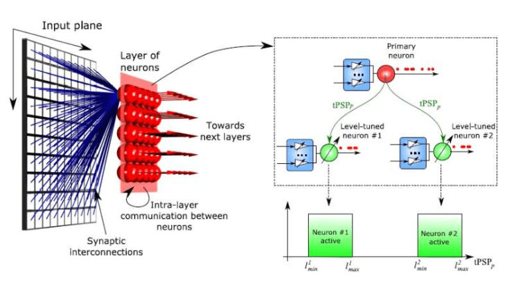
Figure 1. Structure of a neuromorphic computing layer with synaptic interconnections from an input plane to a layer of neurons.
Non-volatile memory (NVM) has been created as the reason for neuromorphic registering since unpredictable irregular access memory (Slam)- put together synaptic activities with respect to CMOS circuits squander energy. Stage change memory, resistive random-access memory (ReRAM), and turn force move irregular access memory (that is, a speck item machine) are a couple of NVM innovations that can at the same time supply memory (that is, a weight stockpiling unit) and rationale units. Among these NVMs, ReRAM cells or memristors offer the benefits of more modest impressions and lower power utilization without forfeiting different variables. Memristive crossbar exhibits have proactively shown a scope of capacities, for example, multi-facet perceptron networks, unaided example characterization, and proficient differential condition arrangements. For edge registering and the Web of Things, where normal handling of simple and computerized information in cell phones limits the need to arrive at the cloud, mixture CMOS memristive circuits seem promising. This is on the grounds that NVM and multi-state exchanging coincide in memristors. Traditional memristors made of mass materials, like progress metal oxides, depend on hierarchical lithographic designing, which has restricted control and tunability over neuromorphic usefulness on the grounds that the gadget's reaction is intensely reliant upon the nuclear scale construction of imperfections. Then again, by making low-layered nanomaterials with an unrivaled degree of control, we exhibit the stoichiometry, imperfection designing, and interfacial science that underlie synaptic capability. Low-layered nanomaterials likewise offer electrostatic tunability, quantum stage changes, novel state factors, and nuclear level control for programmable switches and neuromorphic functionalities. As opposed to zero-layered (0D) and one-layered (1D) nanomaterials, which empower exceptionally delicate covalent functionalization and redox science for multi-bit states, two-layered (2D) nanomaterials in this class of materials offer an open engineering for different terminals, in-situ examining, and spatiotemporal reactions. The results of hybrid systems that mix nanomaterials in several dimensions are equally encouraging. Because of their mechanical flexibility, low-dimensional nanomaterials are assisting in the development of wearable neuromorphic applications such as afferent nerves and intelligent prosthetics. In this article, we review recent advances in the emerging field of neuromorphic nanoelectronics materials with a focus on how the properties of 0D, one dimension, and 2-D nanomaterials and their van der Waals heterogeneous structures enable distinct neuromorphic responses in comparison to organic and inorganic substances whose neuromorphic potential has already been comprehensively reviewed elsewhere.
Zero Dimensional Materials
The optical characteristics of zero layered nanomaterials are impeccably fit to neuromorphic execution in photonic frameworks. Photonic devices provide simultaneous interaction and hyper-connectivity because photon transmission is not constrained by identical spatial and power density restrictions as wires in electrical systems. Sadly, two issues have hampered the advancement of this strategy. To begin with, while direct media are inclined towards optical correspondence, non-direct media are additionally expected to accomplish signal increase. Second, it has been trying to foster viable memory parts that use exclusively optical signs. Because of this, mixed optoelectronic systems are commonly utilized in applications where photonics-based communications and memory are possible Using printed using 3D printer diffraction gratings and neural networks, ten thousand objects can be categorized with a precision of more than 80%. Then again, 0D semiconducting quantum dots (QD) offer clear energy levels for optical handling, though zero-layered nanoparticles of metal have size-tunable plasmonic reactions that empower neighborhood gain. In this fashion, excitatory and inhibiting synaptic responses have been successfully mimicked by mode-locked lasers based on InAs/InGaAs QDs. Although the operating principle is made easier in this situation by the multi-band emission of QDs, colloidal QD integration with photonic wave guides is still challenging. By and by, electro-photosensitive memristors with conductance constrained by either electrical or optical heartbeats have been created utilizing site-controlled quantum spots on GaAs/AlGaAs wafers. Base up QD amalgamation yields molecularly exact size, shape, and compound structure, prompting definitively controlled actual reactions. For instance, CsPbBr3 perovskite colloidal QDs coupled to natural semiconductors show present moment as well as long haul adaptability in response to electric and visual boosts. ReRAM can likewise be achieved by blending QDs and metallic nanoparticles into an inorganic or natural lattice. It has proven feasible to produce printed multiple levels ReRAM with a significant changing rate, where charges trapped in the black phosphorus QDs facilitates filament production and rupture, by sandwiching them between poly (methyl methacrylate) bilayers. Indistinguishable charge catching in Au nanoparticles in view of pentacene sheets has been utilized in synaptic semiconductors. Small compounds, such as metal-composed azo-aromatics, occasionally have benefitting zero dimensional properties that are comparable to those utilized in commercial inorganic ReRAM measurements.
Conversely, memristor fibers ordinarily approach the nanoscale aspects that in the end uncover 0D nature. The diffusive memristor is a conspicuous case of 0D Ag nanoparticles been deliberately brought into a SiOx grid. These Ag nanoparticles show dynamic withdrawal and augmentation due to contending impacts from the surface pressure and the electrical field, prompting in viable learning behavior. One more use for semiconductor QDs is in quantum memristors that use Josephson intersections, by which the variety in stage between semiparticles goes about as a state variable. These gadgets can dispose of the unavoidable stochasticity present in regular deformity based memristors, notwithstanding the way that the memristive circle is anticipated to be moderately small. Quantum brain frameworks and other neuromorphic models have additionally been developed in light of QD clusters. In the setting of assembling issues, metal oxide memristors had been scaled to the degree of sub-5 nm paths with slender pitch (6 nm), which imitates the fundamental QD exhibit structure. Be that as it may, a quantum brain network should likewise show quantum lucidness between QDs to be totally understood, notwithstanding the fundamental condition of quantum being acknowledged in high-portability semiconductors rather than metal oxides.

To learn about use of graphene sheets in nanoelectromechanical systems (NEMS), you can read our blog.
One Dimensional Materials
Early interest in 1D nanomaterials for neuromorphic applications was sparked by their topological resemblance to tubular axons, which is required for excessive connectivity in biological systems. Moreover, 1D nanomaterials can be utilized in gadgets because of their large number of physical and compound qualities, versatile base up creation, and arrangement processability. One of the most completely contemplated 1D nanomaterials is the carbon nanotube, a moved up graphitic chamber with a metal or semi-leading way of behaving that relies upon its chiral vector. Due to their significant charge transporter mobilities and gainful scaling properties, semiconductor single-wall CNTs have been investigated for post-silicon advanced rationale, quite at the super short channel range (that is, sub-5 nm hub). Synaptic circuits have likewise been concentrated on utilizing CNT semiconductor models. The topological similitude of 1D nanomaterials to rounded axons, which is fundamental for unnecessary association in organic frameworks, initially provoked interest in them for neuromorphic applications. Also, due to their various physical and chemical properties, versatile base up union, and arrangement processability, 1D nanomaterials can be utilized in gadgets. The carbon nanotube, a wrapped-up graphitic chamber with metallic or semi-conducting properties based on its chiral vector, is one of the most extensively researched 1D nanomaterials. In particular, at the ultra-short channels limit (i.e., sub-5 nm node), semiconductors single walled CNTs have been investigated for post-silicon digital logic due to their significant charge carrier mobilities and advantageous scaling features. CNT transistor models have also been used to study synaptic circuits.
Two Dimensional Materials
Throughout the past ten years, basic investigation of two-dimensional nanomaterials has paved the way for a number of technologies, which have been previously evaluated. Compared to zero-dimensional and one-dimensional nanomaterials, two-dimensional nanomaterials supply greater device scalability and compatibility with planar wafer technology. Unexpected mechanisms were uncovered during the first attempts to achieve neuromorphic functioning in 2D nanomaterials, which prompted the creation of new device designs. For instance, extremely thin vertical memristors (thickness 1 nm) made of single layer shift metal dichalcogenides (TMDCs) of the type MX2 have a low ON-state resistance (10) that enables high-frequency switches to function at 50 GHz. This high switching ratio (> 104) casts doubt on commonly held beliefs about the currents that leak in monolayer semiconductor and opens the door to novel switching processes, in which point defects are anticipated to play a significant role. Related studies show that van-der Waals connections, or few-layer MoS2 memristors placed between graphene layers, work at temperatures that are much higher (340 °C) than those of conventional metal oxide memristors (200 °C). According to in situ scanning transmission electron microscopy, these memristors exhibit a larger concentration of sulfur vacancies in the ON-state, which are occupied by oxygen ions in the OFF-state.
Nanomaterial Based Transistors and Semiconductors
Nanomaterials for transistors started gaining attention about 15 years ago. The first molecules to receive serious study were carbon nanotubes, which are made up of a single layer of carbon atoms organized in a hexagonal lattice. Its advantages were soon widely recognized. It was clear why interest in nanotubes for electronics exploded given their near-zero resistance capacity to transmit electrical current even at ambient temperature. An associated carbon allotrope called graphene benefited from the widespread enthusiasm that carbon nanotubes had sparked for nanomaterial devices. Although the lack of an energy band gap ultimately made graphene transistors less practical for digital applications, the excitement surrounding the material sparked a complete resurgence in research in other related two-dimensional materials.
Nanoparticles made of semiconductors are fluorescent materials. To minimize photobleaching, silica coating is applied to them. The semiconductor nanoparticles coated with an extra layer of semiconductor have shown to be of significant importance for enhancing the luminous properties of these core-shell assemblies. The shell's composition affects where the electron-hole pair is located. Similar to nanostructures like CdSe/CdS or CdSe/ZnS, the conduction region of the shell material, which has a larger bandgap, is at a higher energy than the core, while the valence band, or valence band, of the shell is at less energy than the core. The center of these materials is the only place where electrons and holes may exist.
Next-Generation Neuromorphic Semiconductors
The goal of neuromorphic computing is to enable the next generation of intelligent gadgets and autonomous systems. Many labs are spearheading research efforts to achieve this goal. Neuromorphic computing, which is based on the concepts of biological neural computation, employs novel algorithmic techniques that simulate how the human brain interacts with the outside world to produce capabilities that are more closely related to human cognition.
Spiking neural networks (SNNs), innovative models that dynamically re-map neural networks to replicate natural learning, are used in neuromorphic computing to respond to patterns that have been learned over time. These asynchronous, event-based SNNs are used by neuromorphic computers to outperform conventional architectures in terms of power and performance by orders of magnitude.
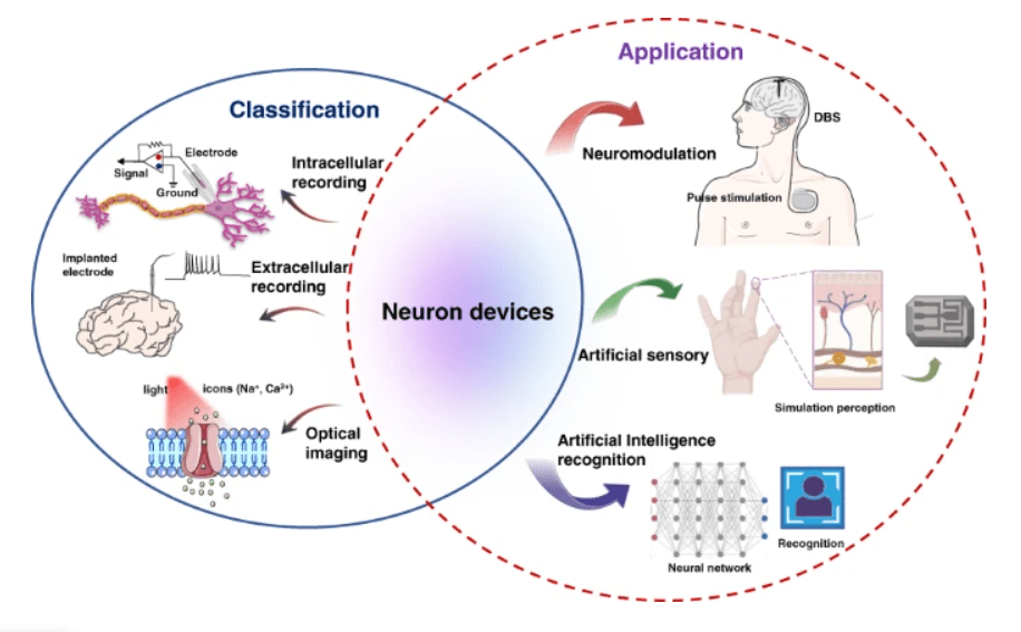
Figure 2. Neuron devices: emerging prospects in neural interfaces and recognition.
Opportunities of Neuromorphic Nanomaterials
To modulate brain tissue, Numerous neuromodulation techniques, ranging from connected devices to nano-scale methods, have been investigated. Controlled electrical modifications of neural activity are frequently used in neuromodulation. One of the most effective methods for treating the clinical symptoms of several neurological illnesses, including Parkinson's Disease, is deep brain stimulation (DBS) (PD). It needs an invasive surgical treatment that carries the possibility of complications despite relieving motor symptoms. In reality, due to hardware issues or infections, 15 to 34% of patients who receive DBS need follow-up operations for electrode removal or replacement. Moreover, the average cost of DBS over 5 years for a patient with PD is US$186. This surgery is therefore underutilized for the eligible patient population because many people are hesitant to undergo it.
As an alternative, several noninvasive neurostimulation methods have been created and put to use, including focused ultrasound, transcranial magnetic stimulation, transcranial direct current stimulation, vagal nerve stimulation, and transcranial alternating current stimulation. Yet, when it comes to deep subcortical areas, these approaches fall short of DBS in terms of targeting accuracy and appropriate penetration. Other neurostimulation methods motivated by material sciences have been proposed to get around these problems and satisfy the growing need for better neuromodulation therapy. Due to their numerous potential applications, newly created milli- and nano-scale devices have been studied in pre-clinical research. When opposed to traditional tethered devices, the key benefit of employing nanomaterials and/or milli-scale devices for neuromodulation is that they may be less intrusive, more affordable, and biocompatible. Here, we use the body of literature that was accessible at the time of writing to highlight the major developments in the use of these technologies.

Challenges of Neuromorphic Nanomaterials
In this segment, we give the ongoing comprehension of the mechanics and specialized difficulties in nanomaterial-based neuromorphic gadgets. Despite the fact that size-subordinate highlights are an almost pervasive theme in the properties of nanomaterials, their importance in neuromorphic frameworks isn't completely obvious. In 2D memristors, for instance, the exchanging proportion changes fundamentally and may sporadically scale with thickness due to contending exchanging systems. There is no obvious connection among speed and thickness, and working voltages range from 0.3 V to 30 V. The way that most of synaptic semiconductors utilize the intrinsically sluggish cycles of charges catching or particle versatility is probably the motivation behind why the reaction time reliably outperforms a millisecond, regardless of the gadget plan or the material utilized. Clearly the gadget estimations in neuromorphic frameworks contain a perplexing arrangement of elements that go against basic plan rules, and total cognizance of the essential actual mechanics is vital to streamline a given framework successfully. Just a chosen handful of components exchanging, such as those in quantum stage shift memristors and QD photonic neurotransmitters, can be totally perceived.
Artificial synapses, neurons and networks
For neuromorphic PC equipment, actual models are expected at three distinct scales,
1-for individual parts, like manufactured neurotransmitters and neurons,
2-for organizations of these neural connections and neurons; and
3-for learning rules and preparing techniques.
A few early investigations of the actual qualities of neurons, gave the establishment to additional progressions in how we might interpret the human cerebrum. Basically, the phone body of a neuron gathers and collects synaptic charges from the dendrites until they arrive at a foreordained level, when the neuron fires a spike along the axon. Neurotransmitters, which can either enhance or block the sign in view of synaptic loads, permit the ensuing spike to be passed to local neurons. A more physiologically accurate Hodgkin-Huxley model, which served as the basis for later approximations, requires paired differential equations such as the concentrations of potassium and sodium ions. Later studies in neuroscience focused on the more abstract principles underlying memory, thinking, and behavioral patterns of neuronal communities; their resulting models later served as the inspiration for ANN architectures (such as Hopfield networks) as well as learning rules (such as Hebbian learning). Although there were hardware implementations before CMOS (such vacuum-tube hardware versions), software ANN application on CMOS equipment rapidly surpassed them because of ongoing increases in energy from integrated circuit shrinking. A renewed interest in reviewing the implementation of hardware has been inspired by the impending incapacity of current systems to handle rapidly rising computational and capacity demands.
For example, assuming information stockpiling and correspondences continue at the ongoing rate, how much power required by double tasks utilizing CMOS would surpass 1027 Joules in 2040, which is bigger than the all-out energy created all around the world. Therefore, examination into lower-energy CMOS options depends on non-von Neumann PC structures. By consolidating the flows from the neurotransmitters, a defective capacitor can be used to shape the least difficult coordinate and-fire neuron, with the spillage current helping with carrying the neuron to a condition of rest. More effective neuron models produce spiking conduct using semiconductor frameworks like Schmitt triggers, summation enhancers, and comparators in light of the fact that capacitors consume a lot of room on chips. The less difficult aspect of the framework is the neural connection, which comprises of only two units: a weight holder and an enlistment methodology unit that changes the load in response to spiking occasions. The first synaptic semiconductor (or synaptic semiconductor) had a drifting entryway where hot electron infusion and burrowing, which changed the device's threshold voltage and conductivity, accordingly, kept or discharged the charge on the hovering gate.
Conclusion
In conclusion, the development of nanoelectrodes using nanomaterials holds promise as a fresh approach to wireless neural devices. Future study is essential to comprehending the potentials and constraints of this technology because this discipline is still in its infancy. Moreover, studies into toxicity, cell/tissue targeting selectivity, and noninvasive delivery methods will advance this technology toward clinical use. Many researchers have examined the neuromodulatory potential of nanomaterials, although the bulk of them have relied on in vitro or silico simulations.
In this context, it is important for nanomaterials to be of high quality and high performance in this promising field. Discover advanced technology nanomaterials with Nanografi today!
CMOS - Vikipedi. (n.d.). Retrieved January 26, 2024, from https://tr.wikipedia.org/wiki/CMOS
Franklin, A. D. (2015). Nanomaterials in transistors: From high-performance to thin-film applications. Science, 349(6249). https://doi.org/10.1126/SCIENCE.AAB2750/ASSET/6C98D3B5-47CD-47D8-A4EF-923165ED786B/ASSETS/GRAPHIC/349_AAB2750_FA.JPEG
Full article: Nanomaterials in neuromodulation: what is the potential? (n.d.). Retrieved January 26, 2024, from https://www.tandfonline.com/doi/full/10.1080/14737175.2022.2056447
Geim, A. K., & Grigorieva, I. V. (2013). Van der Waals heterostructures. Nature 2013 499:7459, 499(7459), 419–425. https://doi.org/10.1038/nature12385
Hodgkin–Huxley model - Wikipedia. (n.d.). Retrieved January 26, 2024, from https://en.wikipedia.org/wiki/Hodgkin%E2%80%93Huxley_model
Knoben, R., Alosaimi, F., Dominguez-Paredes, D., Temel, Y., & Jahanshahi, A. (2022). Nanomaterials in neuromodulation: what is the potential? Expert Review of Neurotherapeutics, 22(4), 287–290. https://doi.org/10.1080/14737175.2022.2056447
Muksuris, K., Scarisbrick, D. M., Mahoney, J. J., & Cherkasova, M. V. (2023). Noninvasive Neuromodulation in Parkinson’s Disease: Insights from Animal Models. Journal of Clinical Medicine 2023, Vol. 12, Page 5448, 12(17), 5448. https://doi.org/10.3390/JCM12175448
Neuromorphic Computing and Engineering with AI | Intel®. (n.d.). Retrieved January 26, 2024, from https://www.intel.com/content/www/us/en/research/neuromorphic-computing.html
Pantazi, A., Woźniak, S., Tuma, T., & Eleftheriou, E. (2016). All-memristive neuromorphic computing with level-tuned neurons. Nanotechnology, 27(35). https://doi.org/10.1088/0957-4484/27/35/355205
Sangwan, V. K., & Hersam, M. C. (2020). Neuromorphic nanoelectronic materials. Nature Nanotechnology, 15(7), 517–528. https://doi.org/10.1038/S41565-020-0647-Z
Semiconductor Nanoparticles - an overview | ScienceDirect Topics. (n.d.). Retrieved January 26, 2024, from https://www.sciencedirect.com/topics/materials-science/semiconductor-nanoparticles
Use of Graphene Sheets in Nanoelectromechanical Systems (NEMS) - Nanografi Nano Technology. (n.d.). Retrieved January 26, 2024, from https://nanografi.com/blog/use-of-graphene-sheets-in-nanoelectromechanical-systems-nems/
Wang, Y., Liu, S., Wang, H., Zhao, Y., & Zhang, X. D. (2022). Neuron devices: emerging prospects in neural interfaces and recognition. Microsystems & Nanoengineering 2022 8:1, 8(1), 1–13. https://doi.org/10.1038/s41378-022-00453-4
Recent Posts
-
 Protection Against Laser")
Advanced Materials for Unmanned Aerial Vehicle (UAV) Protection Against Laser
Consider a UAV on a critical mission, rendered inoperative by a sudden laser attack. With the increa …26th Jul 2024 -

Simulation and Modeling of Material Properties
Our world is composed of a dazzling array of materials, each with its own unique properties that dic …19th Jul 2024 -

Advanced Coatings for Superior Corrosion and Wear Resistance
Corrosion and wear pose significant challenges across various industries, leading to substantial eco …12th Jul 2024