Sputtering: Process, Types, and Uses
Sputtering is a physical process in which atoms in a solid-state (target) are released and pass into the gas phase by bombardment with energetic ions (mainly noble gas ions).
Introduction
Sputtering is usually understood as the sputter deposition, a high vacuum-based coating technique belonging to the group of PVD processes. Furthermore, sputtering in surface physics is used as a cleaning method for the preparation of high-purity surfaces and as a method for analyzing the chemical composition of surfaces.
Process of Sputtering
The principle of Sputtering is to use the energy of a plasma (partially ionized gas) on the surface of a target (cathode), to pull the atoms of the material one by one and deposit them on the substrate.
To do this, a plasma is created by ionization of a pure gas (usually Argon) by means of a potential difference (pulsed DC), or electromagnetic excitation (MF, RF); this plasma is composed of Ar+ ions which are accelerated and confined around the target due to the presence of a magnetic field. Each ionized atom, by striking the target, transfers its energy and rips an atom, having enough energy to be projected to the substrate.
The plasma is created at relatively high pressures (10-1 - 10-3 mbar), but it is necessary to start from a lower pressure before the introduction of Argon, to avoid contamination due to the residual gases.
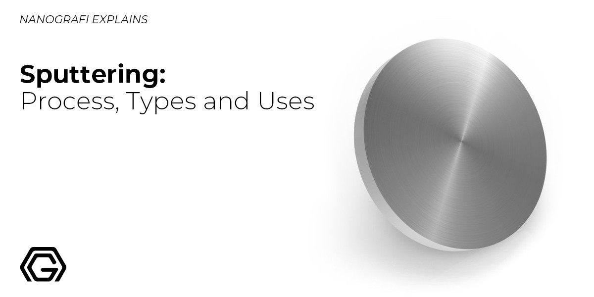
The diversity of sputtering target shapes (circular, rectangular, Delta, tubular...) and the materials used allows creating all types of thin layers, including alloys during a single run.
Basics of the Sputtering Process
When bombarding a surface with ions, various effects may occur, depending on the ions used and their kinetic energy:
1. Material is removed from the bombarded target (cathode). This is the sputtering described here.
2. The ions are incorporated into the target material and enter there, possibly a chemical compound. This effect is then called (reactive) ion implantation.
3. The ions condense on the bombarded substrate, where they form a layer: ion beam deposition.
If a material removal is intended, the ions must have a certain minimum energy. The impinging ion transmits its impulse to atoms of the bombarded material (target), which then - similar to the billiards - trigger further collisions. After several collisions, some of the target atoms have a momentum away from the target interior. If such an atom is sufficiently close to the surface and has sufficiently high energy, it leaves the target.
The sputter yield depends essentially on the kinetic energy and mass of the ions and on the binding energy of the surface atoms and their mass. In order to eject an atom from the target, the ions must have material-dependent minimum energy (typically 30-50 eV). Above this threshold, the yield increases. However, the initially strong increase flattens rapidly, since at high ion energies, this energy is deposited even deeper into the target and thus barely reaches the surface. The ratio of the masses of ion and target atom determines the possible momentum transfer. For light target atoms, maximum yield is achieved when the mass of target and ion approximately match. However, as the mass of the target atoms increases, the maximum of the yield shifts to ever higher mass ratios between the ion and the target atom.
The ion bombardment generates not only neutral atoms, but also secondary electrons and, to a lesser extent, secondary ions and clusters of different masses. The energy distribution of the dissolved atoms has a maximum at half the surface binding energy, but falls to high energies only slowly, so that the average energy is often an order of magnitude above. This effect is exploited in analysis methods of surface physics and thin-film technology as well as for the production of thin layers (sputter deposition).
To get more information about sputtering targets,
you can read our blog post here.
Types of Sputtering
The main types of Sputtering are discussed below:
1. DC diode sputtering
With a DC voltage = 500 - 1000 V, an argon low-pressure plasma is ignited between a target and a substrate. Positive argon ions precipitate atoms out of the target, which then migrates to the substrate and condenses there.
Limitations
Only electrical conductors can be sputtered, as otherwise an opposing field builds up and the sputtering process stops. The other limitation is that only low sputtering rates are achieved since only a few argon ions are formed.
2. RF sputtering
In radio frequency sputtering, a high-frequency alternating field is applied instead of the DC electric field. The necessary high-frequency voltage source is connected in series with a capacitor and the plasma. The capacitor serves to separate the DC component and to keep the plasma electrically neutral.
The alternating field accelerates the ions and the electrons alternately in both directions. From a frequency of approximately 50 kHz, the ions can no longer follow the alternating field due to their much smaller charge-to-mass ratio.
The electrons oscillate in the area of the plasma and there are more and more collisions with argon atoms. This results in a high plasma rate, a consequence of which is the possible pressure reduction to about 10-1 - 10-2 Pa) with the same sputtering rate. This allows the production of thin layers with a different microstructure than would be possible at higher pressures.
The positive ions move through a superimposed negative offset voltage on the target in the direction of the target and solve as in DC sputtering by collision atoms from the target material. The subsequent sputter deposition corresponds to that of other sputtering methods.
Benefits
1. Insulators (e.g. aluminum oxide or boron nitride) and semiconductors can also be sputtered
2. the substrate heats up less
3. Due to the oscillating electrons, the sputtering rate at the same chamber pressure is about 10 times higher than with DC sputtering.
Limitations
1. Relatively low coating rates
2. The RF generation is more expensive than a DC voltage source
3. For large rectangular cathodes (> 1m), unevenness in the plasma density (layer thickness distribution) may occur.
3. DC Triode Sputtering
The target is placed as a third electrode outside the plasma chamber. Plasma generation and sputtering process are decoupled.
4. Magnetron
While in the simple cathode sputtering, only an electric field is applied, an additional magnetic field is arranged at the magnetron sputter behind the cathode plate. Due to the superimposition of the electric field and the magnetic field, the charge carriers no longer move parallel to the electric field lines but are deflected onto a spiral path (exact cycloid orbits) - they now circle over the target surface. This prolongs their path and increases the number of impacts per electron. The electron density is highest at the point where the magnetic field is parallel to the target surface. This causes a higher ionization in this area. Since the ions are hardly deflected by the magnetic field due to their mass, the largest sputtering on the target takes place directly in the area below. The erosion trenches are typical of magnetron sputtering form on the target.
The effectively higher ionization capacity of the electrons leads to an increase of the noble gas ion number and thus also of the sputtering rate. As more target material is atomized, this leads to significantly higher coating rates at the same process pressure. Since the layer growth and thus the layer properties in addition to the temperature depends primarily on the process pressure, you can start with the same growth rates, the process pressure by up to one hundred times lower than in conventional sputtering. This results in less scattering of the material on the way to the substrate and a denser layer.
Magnetron sputtering is the most widely used method in microelectronics for producing metal layers.
5. Reactive sputtering
Reaction gas (e.g., oxygen or nitrogen) is added to the Argon gas. As with the argon gas, ions of the reaction gas are formed, which react with the sputtered layer atoms in the vacuum chamber. The resulting reaction products are then deposited on the substrate surface. Reactive sputtering is available as a DC and HF variant.
Applications of Sputtering Targets
The phenomenon of Sputtering is employed in the semiconductor industry for depositing thin films of different constituents on silicon wafers. The process is also employed in optical applications by depositing a thin layer on glass. The process of sputtering occurs at extremely low temperatures, due to which, it is the perfect method for depositing thin films of different constituents. This application of the Sputtering process is the most important one and commonly used.
The process of Sputtering has various advantages, from which, the one that stands out is that the concentration of deposited film is similar to the raw material. This is unusual, as indicated earlier, the yield of spray is dependent on the atomic weight of the species. This is the reason that the alloy components are expected to be deposited one by one, which must affect the concentration of the deposited film. Although it is factual that the constituents are sprayed at diverse speeds, being a surface phenomenon, the vaporization of a species preferentially enriches the surface with atoms of the remaining ones, which effectively compensates for the difference in abrasion speeds. Thus, deposited films have a similar concentration as of the raw material.
Another use of the sputtering process is the erosion of white material. An example is found in secondary ion mass spectroscopy, in which the target is sprayed at a constant speed. As this occurs, the identity and concentration of the evaporated atoms is determined by mass spectrometry. In this way, the concentration of the examined material can be estimated and enormously low concentrations of impurities can be recognized. In addition, as the spray is attacking deeper and deeper layers, it is possible to obtain a concentration profile depending on the depth.
Conclusion
Sputtering is a physical process in which the vaporization occurs of a solid material by bombarding it by ion energy. This is a process widely used in the formation of thin films on materials, engraving techniques, erosion of white material and analytical techniques. The sputtering is mainly caused by the momentum exchange between atoms and ions of the material, due to collisions. The Sputtering process can be thought of as a pool game at the atomic level, with the ions (white ball) hitting a cluster of densely packed atoms (billiard balls). Although the primary collision pushes atoms further in the cluster, subsequent collisions among atoms can cause a few atoms near the surface being expelled. The number of atoms expelled from the surface per incident ion is the sputter yield and is a significant measure of the efficiency of the Sputtering process. Some factors that influence this parameter are the energy of the incident ions, their masses and those of the target atoms and the bond energy of the solid.
To get more information, you can visit Blografi.
Recent Posts
-
Advanced Materials for Unmanned Aerial Vehicle (UAV) Protection Against Laser
Consider a UAV on a critical mission, rendered inoperative by a sudden laser attack. With the increa …26th Jul 2024 -
Simulation and Modeling of Material Properties
Our world is composed of a dazzling array of materials, each with its own unique properties that dic …19th Jul 2024 -
Advanced Coatings for Superior Corrosion and Wear Resistance
Corrosion and wear pose significant challenges across various industries, leading to substantial eco …12th Jul 2024


