
Properties and Applications and Gallium
As an element, Gallium was first predicted by a Russian scientist named Mendeleev in 1871. According to him, the element should have properties similar to those of aluminum, and should also have an atomic mass of 68 with its formula as Ea203 and gravity, 5.9. These properties later turned out to be very accurate. Also, later on in the century, another French chemist by name Paul Emile Lecoq de Boisbaurdan, who lived between 1838 and 1912, found out after series of research that the metal that was missing in between aluminum and indium was Gallium, and then discovered some spectral line from samples of Sphalerite (a zinc mineral). A lot of impurities including were also discovered in it. Later on, he separated the pure element using electricity in a solution of hydroxide and potassium hydroxide. Ultimately, Gallium proved to be a very valuable element in different sectors due to its peculiar characteristics. This article aims to mainly discuss the properties and applications of Gallium and will also look at its compounds.
Gallium
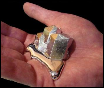
Gallium is not as common as silicon and some other elements, as it can be found in isolated areas like Mars and Uranus. It is used in manufacturing heavy lethal weapons. Unlike other elements, it cannot be found in its form but in the Earth's crust (mineral and ores). When exposed to extreme temperatures, there may be an emission of toxic fumes which may form a corrosive alkaline mixture with water. Gallium particularly has some special qualities. For example, even though at room temperature, it is solid, it is still very soft that you could easily cut it into halves. Gallium is one of the four metals that turn liquid at near room temperature. The other metals are mercury, rubidium, and cesium. Out of these, Gallium is perhaps the least reactive and not as toxic as the others. Thus, making it a good choice for barometers, cooling and heating devices. Gallium has several other benefits, as it covers a wide variety of use.
5 Properties of Gallium
1. Color & Physical State: By its nature, Gallium is a kind of soft metal with a blue-white color combination. Apart from mercury, rubidium, and cesium, it is the only metal that turns to liquid at room temperatures, making it possible to be used in thermometers with high temperature.
2. Vapor Pressure: It has a low vapor pressure at all kinds of temperatures and very long liquid range of any metal.
3. Appearance of Gallium: Pure gallium has a charming outlook and also silvery.
4. Stability and Reactivity: It can only be attacked gradually by mineral acids.
5. Other properties of Gallium: Close to what was predicted by scientist Mendelev, Gallium has an atomic mass of 69.7 approximately; a boiling point of 2204 degrees, melting point of 29.78 degrees and a density of 5.907g/cm3.
Compounds of Gallium
Gallium has different compounds; the main ones are discussed below:
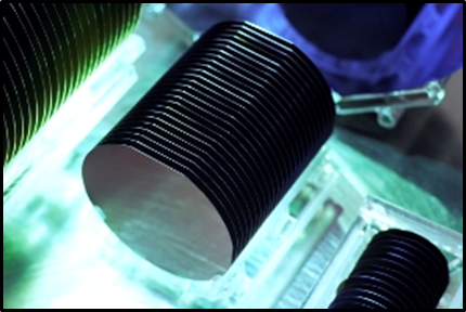
Gallium Arsenide wafers
Gallium Arsenide (GaAs) is a compound which contains Gallium and Arsenic elements. It is a kind of semiconductor with zinc like crystal structure. It is made up of equal amounts of the two elements, gallium, and arsenic. It is very obvious that each atom of arsenic contains up to four gallium adjacent it, while each of the gallium atoms also has about four arsenic adjacent to it, which are lined up in a tetrahedral structure.

Gallium Arsenide which is gotten from a GaAs wafer has the ability to generate laser lights directly from electrical current. Two types of this wafer exist, and they are, single crystal and polycrystalline. Both types are used in the production of micro and opto-electronics for the purpose of creating LEDs, LDs, solar panels, and some other kinds of electronics. Aluminum gallium arsenide (AlGaAs) is used as barrier equipment in GaAs based multi structural devices. This layer limits the electrons to a gallium arsenide region. Furthermore, gallium arsenide can be prepared using three methods or processes:
1. The vertical gradient (VGF) process: Most gallium arsenide wafers are produced through this process.
2. Liquid encapsulated czochralski (LEC) growth: This is mainly used for manufacturing high-purity crystals which can demonstrate partial insulating characteristics.
3. The crystal growth process using a horizontal zone furnace whereby gallium and arsenic vapors react.
Properties of Gallium Arsenide Wafers
- 1.Gallium arsenide has a melting point of 1238 degrees.
- 2.The molar mass is 144.64g/mol.
- 3.Its density is 5.32g.
- 4.It also has a strong garlic smell when moisture is applied.
- 5.It’s only soluble in HCL.
Application and Uses of GaAs Wafers
Gallium arsenide wafers are mainly used in computers, transistors, aerospace, photovoltaic cells, and specific electronics.
1. GaAs Wafers’ Applications in computers and transistors
The use of GaAs wafers is complicated in the production of transistors in the sense it is a binary compound with a lesser thermal conductivity, and a higher thermal expansion coefficient (CTE), while germanium and silicon are the basic semiconductors. Also, it is easier to understand failure in devices built with silicon than those based on Gallium arsenide. Also, its currency in use makes it more expensive than the others.
2. GaAs Wafers’ Applications in Aerospace
Gallium arsenide wafers has been introduced into the market since the inception of its use in the aerospace field.
3. GaAs Wafers’ Applications in photovoltaic cells
Gallium arsenide is used in photovoltaic cells tunnels. It is also used in the production of semiconductors, lasers, and transistors.
4. GaAs Wafers’ Applications in the substrate material
In substrate material, gallium arsenide is used for the growth of other semiconductors (III-V).
5. GaAs Wafers’ Applications in LED
Gallium arsenide devices produce less noise than many other types of semiconductor components. It is partially used in the manufacture of LEDs which are found in control systems and optical communications. Silicon has been the main component used in the manufacture of linear and digital ICs. However, gallium arsenide can replace silicon in such applications since it has some technical advantages over silicon. One of such benefits is that electrons tend to move faster through its crystalline structure.
6. GaAs Wafers’ Applications in optical fiber temperature measurement
An optical fiber is made up of a gallium arsenide crystal. Beginning at a wave length of 850nm, gallium arsenide becomes totally translucent. Since its positioning is dependent on temperature, it shifts about 0.4nm/k. The device comprises a light source and a device used for the detection of the band gap. The changing of the band gap propels an algorithm to calculate the temperature.
7. GaAs Wafers’ Application in other electrical devices
GaAs devices are not affected by overheating, thanks to their wider bandgap. These special attributes and qualities make it the best choice for the production of satellite TVs, microwave circuits, and so on. Another advantage GaAs has over silicon in this regard, is a direct bandgap, thus, making it capable of absorbing and emitting light effectively. On the other hand, silicon does not have a direct bandgap thus, making light emission relatively poor. Due to its wide energy bandgap, pure gallium arsenide is highly resistant. The presence of a high dielectric constant makes it an excellent substrate for integrated circuits. Also, unlike silicon, it provides isolation between circuits and devices, again, making it a perfect material for microwave circuits.
Gallium Antimonide Wafers
Introduction
Gallium Antimonide (GaSb) is a semiconductor (III-V family) comprising gallium and antimony. Its lattice compound is about 0.61mm and a bandgap of 0.67ev. Gallium antimonide can be used to manufacture lasers, transistors, infrared LEDs, photovoltaic systems and other electronics. GaSb can sometimes be distributed as wafers with clearly-cut finishes, and are also available in a variety of carrier concentration.
Properties of Gallium Antimonide
Electrical properties of GaSb
1. Presence of electron mobility is less than 3000 cm³v-1s-1.
2. It has an electron diffusion coefficient of 75cm²s-1.
3. It has the ability to change properties in high electrical fields.
Mechanical properties of GaSb
1. Its melting point is 712°C.
2. The density is 5.614 g/cm³.
3. The Bulk modules is 5.63×10¹¹dyn cm-1.
Optical properties of GaSb
Having an understanding of the optical properties of Gallium Antimonide (GaSb) is important due to its increasing usage in various optical and electronic applications. The properties include:
1. A retractive index of 5.24 (max) at photon energy 2.0eV
2. An extinction coefficient of 413 (max) at photon energy 42eV
3. Dialect constant of 25.6 (max) at photon energy 2.0 eV
4. An absorption coefficient of 1.76×10(8) at photon energy 4.2 eV
Chemical properties of GaSb
1. Its chemical formula is GaSb.
2. Its molecular weight is 191.483 g/mol.
3. It belongs to group III-V.
4. IUPAC name is gallium (III) antimonide.
5. Its band gap is 0.726 EV Angostroms.
Thermal properties of GaSb
1. Its thermal conductivity is 0.32 Wcm-1
2. The Thermal diffusivity is 0.23cm²s-1
3. The Thermal expansion coefficient is 7.75×10⁻⁶.
Applications of GaSb Wafers
1. GaSb wafers are applied as a component in infrared detectors.
2. They are also applied as components of Transistors.
3. They are used in the production of lasers.
4. They are also used in the manufacturing of thermophotovoltaic systems.
Gallium Ingot
An ingot is usually a pure material (mostly metal) which is cast into a shape appropriate for further production or processing. In the process of steelmaking, Ingot is the first step involved in a semi-furnished casting product. They usually require another process of shaping, such as cutting, milling, cold or hot working in order to produce the final product. Semi-conductor and nonmetallic materials prepared in large quantities can also be called ingots, especially when the mold-based method is applied. Also, precious metals can be applied as a currency reserve. Ingots are generally comprised of either pure or alloy metals, which are heated past its melting point and then cast into a block through the mold-chill method.
Gallium ingots are produced through the following processes: crystallization, solid-state and extremely high purification processes like sublimation. Ingots are made out of gallium itself using the above processes. It comes in various shapes such as rods, bars, and plate forms.
Properties of Gallium Ingot
1. Gallium ingot has good casting.
2. Presence of anodic oxidization only in surface protection.
3. Gallium ingot’s corrosion resistance is on the average.
4. The melting range is 525-625°C.
Applications of Gallium Ingot
Gallium ingot can be used as a substitute for silicon in the electronics industry. It forms a vital component of several semiconductors. It is also used in the manufacture of light emitting diodes due to its ability to convert electricity to light. It is also used for making alloys, bars, currency reserve, etc.

Conclusion
Thus, it is evident from the above discussion that gallium has incredibly wide usage. Based on its properties and characteristics, gallium is absolutely safe for humans. In the medical field, gallium alloys are applied in some thermometers as non-toxic substitutes for mercury. As discussed above, Gallium arsenides are utilized in the production of semiconductors majorly for laser diodes, LEDs and solar panels. This particular Gallium is used in the manufacturing process of mirrors.
Recent Posts
-
 Protection Against Laser")
Advanced Materials for Unmanned Aerial Vehicle (UAV) Protection Against Laser
Consider a UAV on a critical mission, rendered inoperative by a sudden laser attack. With the increa …26th Jul 2024 -

Simulation and Modeling of Material Properties
Our world is composed of a dazzling array of materials, each with its own unique properties that dic …19th Jul 2024 -

Advanced Coatings for Superior Corrosion and Wear Resistance
Corrosion and wear pose significant challenges across various industries, leading to substantial eco …12th Jul 2024