
IR Coating Technology and Applications
IR coating technology is used for the optical coatings that perform their functions at a very large scale. This includes UV wavelengths which are both short and long too. A lot of comprehensive studies have been conducted to prove the efficacy of IR coating technology which has been considered extremely beneficial.
There are a lot of applications of IR coating technology as it is an essential part of the industries. All these applications are running thoroughly due to the excellent features that IR coating technology brings to the table. Along with that, it offers a wide range of characteristics that are excellent and highly authentic in their nature consequently making it a lot more important. However, it is necessary to keep a thorough check on the productivity methods as even a slight inconvenience can alter the productivity and that can hinder its true characteristics and properties.
Introduction
Optical coatings have various functions at a large range of wavelengths. Short wavelengths (UV) to long wavelengths (IR) are in this spectrum. Artificial and solar light sources radiate visible and ultra-violet light of high photon energies. Reflected solar and thermally emitted energies are overlapped by the Mid-wave IR (MWIR) regions and Short Wave IR (SWIR) regions. Its temperature is the reason for the emission of energy from the source at LWIR wavelengths.

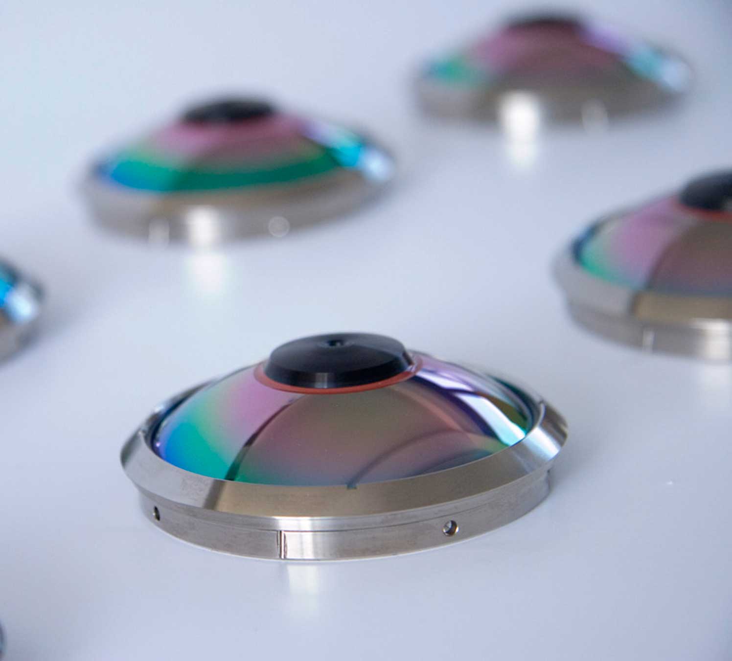
Optical components
The optical components and instruments operating at long wavelengths in the infrared spectrum need various sets of coating materials as compared to those that function at visible wavelengths. A broad range of coating materials can be provided by materion, also the optical coating materials can be determined by our technical experts for meeting our requirements of wavelength.
There is a difference in spectral transmission and the chemical composition of IR materials. IR materials are less mechanically durable as compared to the materials that are utilized in shorter and visible wavelengths. The main aim of this article is on IR coating deposition behavior, their characteristics, the coating materials, and their applications.
IR Coating Materials and Substrates
In chemical composition, they are diverse. This needs special consideration as it is essential for the deposition of durable and functional thin film coatings on their surfaces. Strong bonding and nucleation between the first-coated layer and substrate can be initiated but it often requires an intermediate layer material.
IR Coating Materials
High transmission in the wavelength regions should be possessed by the used IR coating materials and the substrate transmits those high transmissions. In between LWIR and Mid-Wave IR (MWIR) wavelengths, a distinct division occurs in the composition of usable material. At wavelengths of less than ~7000 nm (7 µm), oxide compounds are transparent. High-, medium-, and low- refractive indices are provided by the oxide compound materials and they are needed in the coating’s deposition and their design.
Ge, element group IIB-VIA (ZnSe and ZnS), and fluoride are the corresponding available material choices at more than ~7 µm of wavelengths. High transparency to 10+ µm is displayed by some of the oxide compounds and their mixtures when they are restricted to the thickness of the layer.
Hard wear-resistant coatings
Reactive processes like CVD, produce these very hard wear-resistant coatings, for instance, BP, diamond-like carbon (DLC), and other boron-based compounds. These coatings are not the starting materials.
Thorium fluoride
It has been several decades since LWIR coatings are being made by using thorium fluoride as the low-index material in combination with ZnS. ThF4 is restricted from being used in coating the military optics as it is a radioactive alpha emitter. Alternate non-radioactive compounds are investigated by many groups in the world for finding a suitable substitute for ThF4. Now only some substitute materials are being used, some of them have mechanical properties and transmission similar to ThF4. Oxide compounds can be used to make MWIR coatings, and durable multi-layer coatings can be made from MWIR coatings.
Deposition parameter
For fluoride compounds, the expected parameters for deposition are the following; P ~5 e-06 Torr is the chamber base pressure, ~50 mA is the beam current, 6 kV of e-gun power which is less than the e-gun power that is utilized for the oxide evaporation. The beam should be swept over the material load for being thoroughly melted. Absorbed water can be driven off for forming a uniformly melted evaporation surface and preventing spitting by applying low power for up to four minutes. 10 to 15 Å/ is the evaporation rate.
The temperature of the substrate should be maintained at ~160° C. An uncovered resistance-heated moly boat can alternatively be the evaporation source. As above, melting the charge necessarily requires a slow power ramp-up. It is for all of the fluoride compounds that lower water band depths, higher indices, and higher packing density can consequently result as the higher substrate temperatures approach 200° C. Although when it is paired with ZnS, the growth (condensation) rate of the layers of ZnS is reduced by temperatures higher than ~175° C, therefore causing complications in the accurate monitoring of the thickness.
It should be remembered by the user that such variables as water vapor concentration control, pressure, and pumping capacity will influence the process of the growth of the fluoride film.
Fluoride compounds
In the compounds that have the known LWIR transparency, fluoride compounds are being constantly refined as the starting materials for enhancing their evaporation behavior. During the formation of multi-layer coatings, fluorides cause difficulties due to their potentially problematic characteristics; for instance, tensile stress, low packing density, and water affinity. The mentioned effects can be lessened by the modifications of the procedure's preparation that are underway. YF3 is a material with significantly enhanced behavior.
Growth of fluoride compounds
On exposure of the thin-film layer to the atmosphere, water vapor can occupy the same large void volume that is contained by the columnar microstructure. Fluoride compounds grow with a columnar microstructure. Under low-energy deposition processing like resistance-heated evaporation and E-beam, the structure's dimensions are largest. Sputtering or IAD is used in the addition of impacting energy for lessening the columnar growth dimension.
High tensile stress is also displayed by the Columnar / micro-crystalline microstructure, and stress is often relieved by thick Fluoride coatings for forming tensile crack patterns. Water vapor can simultaneously change the adhesion strength and optical characteristics and permeate the film void volume. Compressive stress is displayed by ZnS and that stress partially compensates for the complete coating design’s total tensile strength.
Thickness
Although, fluoride layers have a thickness of 2/3 of the thickness of the total design in a typical filter making the residual stress, tensile in nature. Mixed materials like IRXÔ have displayed advances in mechanical formation, which formed a Fluoride material and the nanostructure of that fluoride material is dense and amorphous, and thus shallower water bands are displayed by its transmission spectrum. Lower tensile stress and greater mechanical durability are also displayed by it. As compared to pure fluoride, IRX shows more stability under environmental stresses. The production of a more dense (compact) structure is promoted and a large crystallite columnar growth micro-structure is inhibited because of a small % additive.
Coating Designs
When index contrast is large, the coating designs for components like filter advantages. A total thickness of 4-5 µm or large is needed by some of the complex designs, and are therefore prone to high accumulated mechanical stress. It damages the coating’s physical integrity. When there is a large difference in the value of indices, then fewer layers are needed, and lower stress is a result of this thinner combination.
At 10 µm of wavelength, ~1.6 is the index ratio for ZnS/Fluoride combination. ~3 is the index ratio for the Ge/Fluoride combination, which indicates towards advantages of this combination. Although, there is no compatibility of fluoride layers with the Ge surfaces. The binding material's thin layer should be inserted in between these layers, and that causes complications in design. There is compatibility between Ge surfaces and ZnS, and thus ~1.8 of desirable index ratio can be produced. This latter combination of materials has been the basis of various IR designs, with outer layers needing a Fluoride for maximizing the performance (lessening reflectance).
New developments
There have been recent developments in the always increasing amount of applications for IR coatings and infrared (IR) materials. These increasing demands were met by Materion which is a leading supplier and particularly forms and refines infrared (IR) coating materials. Here, we will be reviewing the materials, technology, and some applications that need IR coatings.

If you are interested in MoS2 and PTFE Coatings,
you can read our blog post here.
Basics of IR Technology
Carbon dioxide absorption bands and water in the atmosphere chops us the infrared energy’s spectral regions that reach the earth’s surface, resulting in some particular windows through which the terrestrial IR instruments can function. It’s only in the extraterrestrial space environment that the full solar emission spectrum is available.
Iridium CVD growth
A significant role is played by deposition temperatures and oxygen concentrations in the formation of iridium metal by using Ir (COD) (MeCp). According to assumptions, the overall CVD reaction's growth rate was as following: 65 W = k×p[Ir(COD)(MeCp)]×p[O2 ], the deposition rate constant is presented by k.
Mass-spectrometry analysis
18, 28, 32, and 44, are the mass numbers showed by mass-spectrometry analysis at these temperatures and they correspond to H2O, CO, O2, and CO2. There were assumptions in addition to the O2 /Ir (COD)(MeCp) ratio that the growth rate can be calculated by using a simple plug-flow model of the reactor. This model is mostly made for the tubular hot-wall CVD reactors, the residence time for known gas flow speed (u, cm/s) can replace sample position’s distance (x, cm). So, if the speed of gas flow is higher, the residence time will be shorter. No details of evaluation were provided by the authors unfortunately and they only presented two of the experimental deposition rate profiles and their matching with calculations.
Basic parameters
If we decrease the residence time value, then the thickness uniformity along the length of the reactor can be majorly enhanced. Therefore, O2 /Ir(COD)(MeCp) mole ratio, residence time, Ir (COD) (MeCP) concentration, and deposition temperature are the basic parameters that are important for this process. There was evaluation in the reactor for 5 cm position along with the optimized CVD process conditions, and the evaluation provided a keff value of almost 0.13 cm/s.
Growth rate dependence
The surface of the substrate determines the film growth rate. Differences were shown by Ritterhaus et al. and Sun et al. in the growth of film on TiO2 surface, iridium films, and dielectric materials for instance silicon, Si3N4, and SiO2 too. These dissimilarities are more when it comes to low deposition temperatures.
Correlation of the incubation time duration
In conventional CVD processes, the correlation of the precursor type and the incubation time duration (nucleation effect) can be seen clearly and it can be compared too by utilizing the experimental data that was attained by Kawano et al. Following precursors; Ir(EtCp)(COD), Ir (EtCp) (CHD), and Ir (EtCp) (C2H4) is used under the same conditions like other processes (SiO2/Si substrate type, oxygen concentration 20 %, and deposition temperature 250 °C) for presenting data. The link between the decomposition temperatures of the same precursors that the DSC estimates and nucleation delay is allowed by these data. Nucleation delay’s correlation (minutes) with decomposition temperature looks obvious.
Iridium thin film CVD from other precursors
There were attempts for proposing the formation mechanisms of iridium film from IrH(PF3 )4 and IrCl (PF3)2. The proposed mechanisms can be known as only references as there was not enough experimental data in both cited references so highlighting it is important. Deposition rate's temperature dependence of nitrogen ambient shows an abrupt increase when numerical data is used. This is more pronounced for oxygen ambient. This type of growth is too fast to be used in the practice. PF3 desorption from the growing film’s surface limits the deposition of Ir films that utilize [IrCl (PF3)2 as a precursor, that limitation is most possibly the cause of the strong interaction of PF3 side-product on the metallic surface of IR.
Oxidization
Oxygen is consequently utilized as a co-reactant gas and it also oxidized this phosphine. This co-reactant can be used to lower the Ir film growth’s activation energy and minimal needed deposition temperature, and to increase the growth rate. IrH (PF3)4’s heterogeneous reaction was as following: IrH (PF3)4 (g) ◊ Ir (s) + H2 (g) + 4 PF3 (g). This scheme is basically in comparison with the proposal made about PF3’s strong adsorption.
Iridium growth by ALD
Ir (MeCp) (CHD) and Ir (EtCp) (COD) are the two types of precursors that have been analyzed for the ALD thin film deposition. Today, even if we include these references, there have not been enough suggestions regarding reaction mechanisms yet. The following main characteristics: - in comparison with Ir (acac)3, cyclo-dienyl type precursors displayed much higher deposition rates at the same deposition temperatures; - it should be highlighted that the substrate type determines the deposition rate and it can be evaluated: Ir > Ta, TiO2 and W > Si > SiO2.
Studies have been performed by Hamalainen and coworkers by using oxygen and ozone-hydrogen sequence pulses, following published methods. Deposition rate temperature dependence’s severe shift with hydrogen and ozone as co-reagent is allowed by comparing data.
Applications of IR
It's the long-wave and mid-wave spectral regions where most of the IR applications take place and thermal energy crosses the visible solar energy background. The emitted energy is detected from the sensors and instruments for these regions rather than reflected energy. The applications of IR instruments are growing in number and the expectation is that they will grow more and various IR sensors are produced and brought to the market. Those materials are under continuous development that is utilized in the development of thin-film coatings for these applications.
The following comes in the list of its applications:
- Commercial and military intrusion detection for security; detecting heat sources like personnel and vehicles under camouflaged and nighttime conditions.
- Rescue and Fire searching under nighttime and smoke restrictions.
- Invisible communications, day or night time.
- Automobile night vision: avoidance and detection systems.
- Remote mineralogy: Planetary surface’s composition.
- Climate monitoring: Determines atmospheric gases’ concentration and distribution, those gases include land, ocean, and water vapor temperature mapping through satellite.
- Commercial and Industrial: process the monitoring of the temperature and detect the heat loss points from the buildings.
- Biomedical thermography: monitoring and detecting circulation problems and tumors. Radiation-less and Non-invasive imaging of circulatory blockage and breast cancer.

If you are interested in 2D Nanomaterials Beyond Graphene,
you can read our blog post here.
Applications of IR-based CVD Coatings in Electronics
Earlier, there have been discussions on some of the technological applications of iridium thin films along with the presentation of some of the examples of biological applications. IR-based thin film implementation for instance nanotechnology, electronics, porous and fiber materials covering applications, are some of the examples that have been recently discussed. Here, the focus is on the characteristics of the growth of thin-film on complicated 3-dimensional structures that is significant for applications in nanotechnology and microelectronics.
Data Analysis
The obtained data from some of the works will be analyzed below where there is a presentation of the film conformality data for this purpose. An extremely significant parameter for modern applications of all CVD processes' types is film conformality. The fast increase in the complexity of the device structure is the real problem here. One can present a structure of a device covered with a film in the simplest case. A simplified rectangular-shaped structure's basic well-adapted feature is the aspect ratio, AR=H/G. These are not enough features for modern device structures. Step coverage is used to characterize the quality of the film on the device structures, and it is displayed as d2 /d1 (in percent).
Quantitative methodology
Vasilyev et al. studied the quantitative methodology of thin-film conformality evaluation for various CVD thin film processes and a link of the effective constant of the deposition rate keff with AR, including the step coverage data point that's attained for high-temperature P-CVD ruthenium thin film. Film conformality’s clear dependence can be seen on keff in 0.1-10 cm/s range for
High-speed CVD processes with the decrease to approximately zero. 0.13 cm/s of value is given by evaluating the kinetic data that's displayed in the most informative published work. Allowing the expectation of good film step coverage.
ALD processes
Although, low deposition rate processes consistently include ALD processes too, and such curves are not extremely beneficial because all of the values are close to 100 percent conformality. For ALD processes, the film conformality has been evaluated in various cases by utilizing as d2/d3 ratio (in percent). A new parameter known as ‘structure complexity, SC=AR/G, was introduced by Vasilyev et al. for characterizing the ALD processes, which is very tight than AR and it is more beneficial to analyze aggressive (narrow and deep) device structures. ALD processes can be correctly characterized for some thin films like ruthenium films by utilizing this parameter.
Results
According to the data, the ALD method generally offers better step coverage results than CVD. With a 35 value, the structural complexity is roughly the highest one that's allowed for attaining 100 percent of step coverage. As the temperature and the content of oxygen in the gas mixture increase, the data for CVD worsens, and it indicates reaction shifts to the gas-phase limited conditions. Another observation is that in comparison with the iridium metal films, much worse step coverage is displayed by oxide thin films.
Conclusion
Being one of the most used technologies, IR coating technology is offering some of the best applications to our industries and adding up to the successes that it brings along. This has been possible due to the phenomenal characteristics and features of the IR coating technology that enable the usage of these applications throughout the world in various industries.
To get more information, you can visit Blografi.
References
https://pubs.rsc.org/en/content/getauthorversionpdf/c5ra03566j
https://www.researchgate.net/profile/Janghoon-Park-2/publication/300423582_Roll-to-Roll_Coating_Technology_and_Its_Applications_A_Review/links/5b16b84aa6fdcc6d3e04c93b/Roll-to-Roll-Coating-Technology-and-Its-Applications-A-Review.pdf
https://materion.com/resource-center/newsletters/coating-materials-news/coating-materials-and-technology-for-long-range-ir-coatings
https://materion.com/resource-center/news-archive/microelectronics-and-services/ir-coating-designs-and-applications
Wu, W. P., & Chen, Z. F. (2017). Iridium coating: Processes, properties, and application. Part I. Johns. Matthey Technol. Rev, 61, 16-28.
Recent Posts
-
 Protection Against Laser")
Advanced Materials for Unmanned Aerial Vehicle (UAV) Protection Against Laser
Consider a UAV on a critical mission, rendered inoperative by a sudden laser attack. With the increa …26th Jul 2024 -

Simulation and Modeling of Material Properties
Our world is composed of a dazzling array of materials, each with its own unique properties that dic …19th Jul 2024 -

Advanced Coatings for Superior Corrosion and Wear Resistance
Corrosion and wear pose significant challenges across various industries, leading to substantial eco …12th Jul 2024