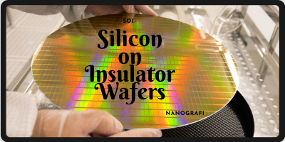
Silicon on Insulator (SOI) Wafers
SOI wafers are long-standing structures that have recently attracted attention in electronic applications.
SOI wafers have offered valuable solutions to the drawbacks of bulk silicon. Excellent properties of SOI wafers are utilized in CMOS/SOI circuits, high frequency applications, and MEMS devices. Silicon has been an important part of technological devices. However, as technology improved the requirement for much more efficient yet smaller devices have increased. Silicon has becom
e inadequate for such needs.
Introduction
Silicon-on-insulator (SOI) structures attracted special attention because they offer solutions to the electrical problems of traditional bulk silicon devices associated with junction area, leakage current, isolation, and parasitic capacitance.SOI wafers are precisely engineered multilayer semiconductor/dielectric structures that provide new functionality for advanced Si devices. The monolithic semiconductor circuits with dielectric isolation instead of junctions are constructed by using SOI wafers.
Characteristcs of Silicon-on-Insulator Wafers
SOI structures consist of a film of single-crystalline Si separated by a layer of SiO2 from the bulk substrate. SiO2 layer is often referred to as the buried oxide (BOX) layer and plays a critical part in SOI structures. Some of the advantages of SOI wafers to traditional bulk silicon are; dielectric isolation, vertical junctions, flexibility in circuit design and processing, short-channel effects, low voltage operation, and reliability. The vertical isolation protects the thin active silicon layer from most parasitic effects induced by the very ‘‘bulky’’ substrate: leakage currents, radiation-induced photocurrents, latch-up effects, etc. On the other hand, the lateral isolation makes inter-device separation in SOI free of complicated schemes. Buried oxide layer reduces junction surface, lower leakage current, and junction capacitance. These conditions result in lower power consumption, improved speed, and wider temperature range. One of the most important aspects of SOI wafer is its potential for scalability. Unlike bulk Si, the film thickness of the SOI wafer is tunable. Moreover, the limited extension of drain and source regions restricted by the small junction area and by the dual-gate control of the body potential makes SOI devices less vulnerable to short-channel effects (SCE), which originates from 'charge sharing' between gate and junctions.
However, there are still some problems with the effective use of SOI wafers. The main problems are the optimization of wafers in terms of cost, uniformity, and availability, specific transistor effects, such as floating body, self-heating, dynamic transients, and interface coupling, and the customization of technology and the design of integrated circuits for SOI applications.
Fabrication Methods of SOI Wafers
Different methods for the fabrication of SOI wafers have been developed over the years resulting in different SOI structures. These methods include; silicon-on-sapphire (SOS), Epitaxial lateral growth (ELO), zone melting recrystallization (ZMR), full isolation by oxidized porous silicon (FIPOS), separation by implanted oxygen (SIMOX), and wafer bonding.
SOS approach involves the epitaxial growth of Si film on Al2O3. The disadvantage of SOS films is the effect of lateral stress, the non-homogenous region in the film, and defects at the interface. However, it is possible to overcome these problems through solid-phase epitaxial regrowth and re-epitaxy. 6 inch SOS wafers covered by 100 nm thick films are available with this technique.
ELO method uses the growth of a single crystal film from a Si substrate on the oxide layer. A further thinning of the Si layer is required for this method which is usually achieved through a post epitaxy process by using a patterned oxide. In the ZMR method, a polysilicon layer is deposited on the BOX and is recrystallized by using a source of energy such as laser, strip heaters, e-beams, and lamps. FIPOS method selectively transforms a part of the silicon layer into the buried oxide layer through an anodic reaction for polymerization and oxidation.
SIMOX is one of the dominants methods for SOI wafer production. This method involves internal oxidation during the deep implantation of oxygen ions into a Si wafer. In order to restore the crystalline quality of the film temperatures as high as 1320°C are used for the annealing process. SIMOX wafer offers good thickness uniformity, low defect density, sharp Si-SiO2 interface, robust BOX, and high carrier mobility. SIMOX provides several different configurations such as thin and thick Si films, low-dose SIMOX with a 100 nm or thinner BOX, standard SIMOX with 0.2 μm thick Si film, and 0.4 μm thick BOX, double SIMOX which involves a sandwiched Si layer between two buried oxide interconnects, and interrupted oxides.
Another important method for SOI fabrication is the wafer bonding method. The oxidized silicon wafer is merged with a second Si wafer for wafer bonding. Then the Si layer is thinned to the desired scale. For this method, Etch-stop layers are required and usually obtained by doping, epitaxy, or by using porous silicon. A specialized form of the wafer bonding process is UNIBOND. The difference between traditional wafer bonding is the absence of the etch-back process. The wafers are separated with the help of natural hydrogen microcavities after bonding and annealing. This method is also referred to as the Smart Cut approach and offers several advantages such as no need for etch-back step, high-quality wafers, the use of conventional equipment, relatively inexpensive wafer production, and a wide range of BOX and thin-film combinations. The resulting wafers have low defect density, good electrical properties, and quality BOX layer.
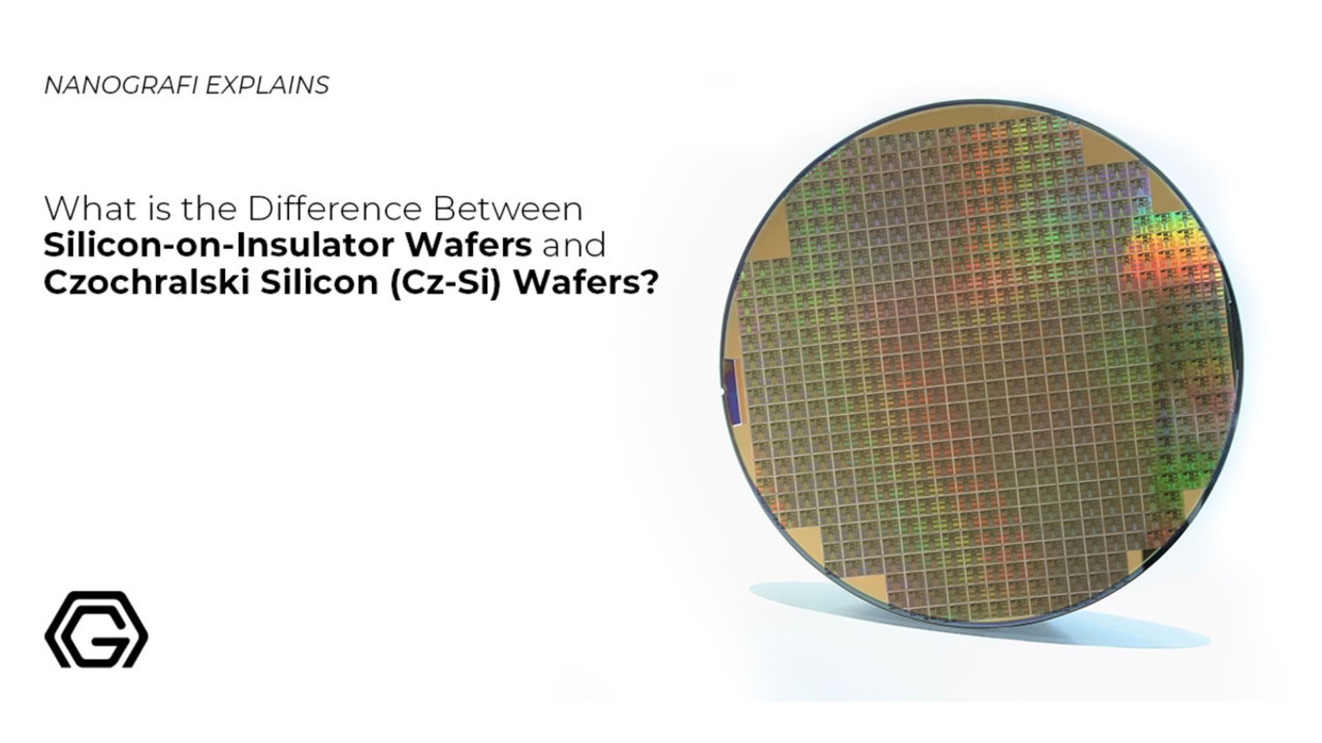
If you are interested in the difference between types of silicon wafers,
you can read our blog post here.
Applications of SOI Wafers
CMOS Circuits
Complementary metal-oxide semiconductor (CMOS) technology has been an important tool to satisfy the needs of ever-evolving technology. Today the semiconductor industry considers Si-based CMOS as a standard RF device technology. Fully depleted CMOS/SOI circuits are used in a wide range of operations with its operational temperatures beyond 300 °C. These circuits are very attractive for oil, aeronautics, and automobile industries. The leakage current of fully depleted CMOS is much smaller and the threshold voltage is less temperature-sensitive (~>0.5 mV/°C) than in bulk Si. Partially depleted CMOS is also popularly used in the digital industry at a 25 nm scale providing high performance, low power alternatives to bulk silicon. The further need for a smaller device, higher operational speed, and low cost for CMOS circuits has promoted the use of SOI (Metal Oxide Semiconductor Field Effect Transistor) MOSFET technology. MOSFET technology for silicon-on-insulator (SOI) has demonstrated its ability for high frequencies and industrial applications in harsh environments (high temperature, radiation). Different SOI MOSFET configurations such as ultra-thin body (UTB) MOSFETs, Strained MOSFETs, Schottky barrier MOSFETs, and multi-gate MOSFETs have been developed to further enhance the performance of CMOS circuits.
UTB and ultra-thin BOX (UTBB, UTBOX or UTB2) SOI MOSFETs are widely considered to be amongst the most promising candidates for the ultimate device scaling thanks to their immunity to short channel effects. Furthermore, UTB SOI MOSFETs offer a reduction in self-heating effect and the use of back-gate control schemes. Strained MOSFETs utilize strained SOI wafers to improve the carrier mobility. Low Schottky barrier contacts are seen as a very interesting candidate for lowering source/drain (S/D) contact resistances, and to form abrupt junctions (with no overlap capacitance) and drastically reduce the thermal budget of the CMOS process. Thanks to the simultaneous control of the channel by more than one gate, multiple-gate architectures emerge as one of the most promising novel device structures to reduce the SCE in nanometre-scale MOSFETs. Different types of multi-gate MOSFETs are available including FinFET, triple-gate (TG), pi-gate (PG), quadruple gate (QG), omega-gate ( Ω -G), and so on. All of these structures are based on different configurations of SOI wafers.
Furthermore, SOI wafers are used for combining CMOS electronics and MEMS devices to obtained enhanced MEMS applications in terms of accuracy. The use of SOI wafers simplifies the manufacturing methods of MEMS and aids the integration of microelectronics and MEMS devices. Additionally, the buried oxide layer in SOI wafers offer several benefits for the traditional microelectronics device industry, such as increased transistor switching speed with reduced power consumption, as well as reduced latch-up. MEMS devices with SOI wafers are being used to construct accelerometers and gyroscopes.
Bi-polar and High Voltage SOI Devices
Thin-film bipolar transistors, with lateral configuration, and BiCMOS circuits have high cutoff frequency while Hybrid MOS-bipolar transistors show increased current drive and transconductance. Lateral double-diffused MOS transistors (LDMOSFETs) are another configuration with a long drift region. The voltage of LDMOSFETs can reach up to 90 V- 1.3 A. Vertical DMOS can be accommodated in thick-film SOI. Using a local buried oxide vertical power devices (LDMOS, IGBT, UMOS,) are located in the non-SOI section of the wafer, whereas a neighboring low-power CMOS/SOI circuit infuses intelligence in the whole circuit. Smart power devices using these bulk Si/SOI structures with 600V/25A are available for high voltage applications.
The wide range of SOI devices also includes optical switches, waveguides and modulators, microwave transistors integrated on high resistivity SOI wafers, and various 3D circuits such as inverters with superposed n- and p-channel transistors.
Conclusion
Silicon-on-insulator technology is a long-standing technology that has gained importance in the last decades. The need for high-performance electronic devices with smaller sizes and higher speeds has accelerated the development and the use of SOI wafers instead of bulk Si in the electronic industry. SOI wafer is consists of Si film separated from the bulk Si layer by a buried oxide layer (BOX). SOI wafers demolish the disadvantage of bulk Si such as leakage currents, radiation-induced photocurrents, latch-up effects while providing scalability and lower vulnerability to short-channel effects. SOI wafers have promoted the development of SOI MOSFET technology which is highly useful in different electronic applications. These advantages of SOI wafers are widely utilized in CMOS/SOI circuits, bipolar and high voltage SOI devices, and MEMS devices.
To discover the latest news from nanotechnology, you can visit Blografi.
References
1.Kononchuk, O., & Nguyen, B. Y. (2014). Silicon-on-insulator (soi) technology: Manufacture and applications. Elsevier.
2.Celler, G. K., & Cristoloveanu, S. (2003). Frontiers of silicon-on-insulator. Journal of Applied Physics, 93(9), 4955-4978.
3.Cristoloveanu, S. (2001). Silicon on insulator technologies and devices: from present to future. Solid-State Electronics, 45(8), 1403-1411.
4.Sawyer, W. D., Prince, M. S., & Brown, G. J. (2005). SOI bonded wafer process for high precision MEMS inertial sensors. Journal of Micromechanics and Microengineering, 15(8), 1588.
5.Cristoloveanu, S., & Balestra, F. (2003). Silicon on insulator: technology and devices. In Advanced Semiconductor and Organic Nano-Techniques (pp. 325-365). Academic Press.
Recent Posts
-
A New Approach to Obesity with Nanotechnology
Obesity stands out as a complex global health crisis that significantly increases the risk of chroni …1st Nov 2024 -
Graphene is the Word in Bionic Technology: EGNITE
Neuroprosthetic technologies have made significant advancements in recent years to enhance the qual …25th Oct 2024 -
MXenes from MAX Phases
MXenes, a group of two-dimensional materials derived from MAX phases, are gaining significant tracti …19th Oct 2024


