Graphene Nanoribbon Synthesis for Advanced Quantum Devices
Graphene nanoribbons with atomic-level precision draw a lot of attention and interest more specifically because of their remarkable tunability in transport, optical and electronic properties.
The synthesis of graphene nanoribbons based on the on-surface synthesis approach is according to the chemical reactions which are basically assisted by the metal surface on which metallic substrates profoundly screen designer electronic properties and restrict even more applications.
Introduction
In order to get over the problem, a new synthesis of on-surface synthesis approach is suggested to achieve graphene ribbons with an atomic-level precision directly on semiconducting metal oxide surfaces. The transformations triggered in multi-steps are pre-programmed in precursors and depend on highly sequential and selective activations of carbon bromine and carbon-fluorine bonds and cyclodehydrogenation.
On-Surface Synthesis Dependence on Instrumentation
Scanning tunneling microscopy is considered a critical technique to help the project achieve success in terms of manipulating the precursor material and evaluating the final results. Scanning tunneling microscope makes it possible to directly prepare SEM micrographs and manipulate material at atomic scales. In so doing, these microscopes are equipped with a needle which is so fine to be equal to the size of a single atom. These microscopes could move on the surface so precisely and line by line to constantly measure any possible infractions between the surface understudy and render atomically accurate topography of surface structure. In the previous studies for achieving graphene nanoribbons, the material was used to be synthesized on a metallic substrate to suppress any possible electronic properties of nanoribbons.1
Mechanism of Action and Applicability
In terms of application, employing a metal substrate has shown to cause problems since it screens the properties. Therefore, the current approach which functions based on the coupling involves the removal of the system from the ultra-high vacuum conditions as well as placing it taking the advantage of a multi-step wet chemistry process. This basically requires etching the metal substrate away which in turn contradicts the accurate and favorable precision employed in creating the system. In this technique, oxide services are experimented in order to find a capable process to function on a non-metallic substrate with the ability to mimic strategies used on metal. In fact, on-surface synthesis makes it possible to obtain materials with high precision which basically comes true when molecular precursors are employed. Moreover, the reactions are necessarily programmed into a precursor where the temperature at which the reaction takes place is known. Another important advantage of these o-surface synthesis is the possibility of employing an extensive range of candidate materials as precursors with a high level of programmability.1 The exact application of reagents to decouple the system sustains an open-shell structure providing researchers with atomic-level precision in order to evaluate molecules with unique quantum properties. Particularly, it is favorable to find out graphene nanoribbons possess magnetic states called the quantum spin states. These conditions and magnetic properties provide a platform to investigate contractions of magnetic fields so that creating qubits for applications in quantum information size comes.
Graphene Nanoribbons
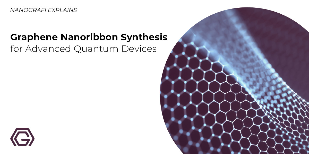
Graphene nanoribbons as one-dimensional strips of graphene have emerged to be the promising candidates to make the future of electronic devices because of their magnetic properties and unique electronic behavior. The lateral size and the edge geometry of graphene nanoribbons give rise to the intriguing properties of the bandgap opening at the Dirac point. Up to this point, heteroatom doping of graphene nanoribbons has been carried out using boron, sulfuric and nitrogen at the edges and very little embedded in its structure. Among the different doping atoms, nitrogen has turned out to be an interesting agent to dope graphene nanoribbons because of its particular electro-accepting characteristics and the affinity to trigger robust ferromagnetism in graphene. In addition to the doping and chemical functionalization, the magnetic and electronic properties of graphene could be modified via creating some pores or defects. With the emergence of surface chemistry, the design and synthesis of doped carbon structures has made a lot of progress in techniques and methodology. Nitrogen-doped graphene ribbons (N-GNRs) with their porous structure exhibit practically desirable magnetic properties as the first-ever porous ladder-like graphene in which some certain carbon atoms in the crystal lattice are replaced with nitrogen atoms.
To learn more about properties of silicene,
you can read our blog post here.
Contributions of Graphene's Properties
Graphene is a rigid two-dimensional (2D) monolayer allotrope of carbon shaped like a hexagonal lattice with a thickness of as much as one carbon and a regular carbon-carbon bond distance of 0.142 nm. Compared to usual three-dimensional materials, graphene shows a rather different electronic structure. In the undoped graphene (pure and not modified), the Fermi level is situated at the connection points (known as Dirac points) of six double cones where its states density falls to zero. This causes the electrical conductivity to be pretty low. However, the Fermi level can be altered through applying an electric field in order to make the graphene electron-rich (n-doped) or porous (p-doped) based on the polarity of the electric field. The doped graphene has potentially higher electrical conductivity than copper at room temperature.2 As one of the most transparent materials, 97.7% of the incident light in the optical region can go through graphene while a normal glass used in windows has a transparency of 88 to 90 percent. Unlike other low-temperature 2D materials, graphene can retain its 2D properties at room temperature. It is 200 times as strong as steel and only one gram of that is enough to cover one football pitch and, in the meantime, it is among the most pliable materials. Like a rubber band, graphene can be stretched 20% while maintaining its electrical conductivity, whereas, silicon, which is widely used in electronics, can only be stretched only 1 percent of its length. This super-material is 10 times more conductive than copper. All in all, graphene is one of the very few materials which is transparent, conductive and flexible.
Graphene Nanoribbons and Quantum Devices
Recently, based on the efforts of an international research project, graphene nanoribbons have been synthesized as ultra-thin strips of carbon atoms growing on a titanium dioxide surface taking advantage of the atomic-level precision with perspective application to go beyond the barriers for designing nanostructures of carbon required for quantum Information science. Graphene could be employed in devices that fall into the nanoscopic scale when they are designed and nanoribbons. Nevertheless, the top-down synthetic method lacks any atomic-scale precision for preparing nanostructures to meet the standards of the current state-of-art applications. To get over the problem, a novel bottom-up technique has been developed to synthesize graphene nanoribbons at the atomic level so that they could be employed in some particular applications.
Conclusion
The practically atomic-level precise technique helps obtain monolayer graphene's unique properties when it is segmented into much smaller parts. It has been demonstrated that only a difference of two atoms in divisive graphene can change its characteristics and properties so considerately leading to the production of metallic ribbon on a semiconductor.1
To discover the latest news from nanotechnology, you can visit Blografi.
References
Cuprous (Copper) Oxide Properties and Applications - Nanografi Nano Technology. (n.d.). Retrieved April 29, 2024, from https://nanografi.com/blog/cuprous-copper-oxide-properties-and-applications/
Electrical and Optical Properties of Silicene: Graphene’s Twin Sister - Nanografi Nano Technology. (n.d.). Retrieved April 29, 2024, from https://nanografi.com/blog/electrical-and-optical-properties-of-silicene-graphenes-twin-sister/
Graphene Nanoribbons - Nanografi Nano Technology. (n.d.). Retrieved April 29, 2024, from https://nanografi.com/blog/graphene-nanoribbons/
Kolmer, M. et al. Rational synthesis of atomically precise graphene nanoribbons directly on metal oxide surfaces. Science (80-. ). 369, 571–575 (2020).
Nitrogen-Containing Graphene Ribbons - Nanografi Nano Technology. (n.d.). Retrieved April 29, 2024, from https://nanografi.com/blog/nitrogencontaining-graphene-ribbons/
Royal, T. H. E., Academy, S. & Sciences, O. F. compiled by the Class for Physics of the Royal Swedish Academy of Sciences Graphene. 50005, 0–10 (2010).
Recent Posts
-
Use of Carbon Nanotube in Touch Screen Technologies
Carbon nanotube (CNT)-based transparent electrodes offer flexibility, durability and cost advantages …8th Nov 2024 -
A New Approach to Obesity with Nanotechnology
Obesity stands out as a complex global health crisis that significantly increases the risk of chroni …1st Nov 2024 -
Graphene is the Word in Bionic Technology: EGNITE
Neuroprosthetic technologies have made significant advancements in recent years to enhance the qual …25th Oct 2024


