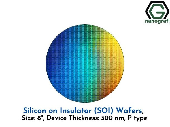
Silicon on Insulator (SOI) Wafers, Size: 8'', Device Thickness: 600 nm, P type
- SKU:
- NG09SIOW0905
Description
1 piece/1152 €
5 pieces/5364 €
Please contact us for quotes on larger quantities !!!
Silicon on Insulator (SOI) Wafers
Size: 8'', Device Thickness: 600 nm, P type
Technical Properties:
|
Size (inch) |
8” |
|
Thickness (μm) |
725 |
|
Resistivity |
1-100 ohm.cm |
|
Grade |
Prime |
|
Dopant |
P type (Boron doped ) |
|
Orientation |
100 |
|
Device Thickness |
600 nm |
|
Device Resistivity |
1-100 ohm.cm |
|
Device Type |
P type (Boron doped ) |
|
Device Orientation |
100 |
|
BOX Thickness |
2000 nm |
Fields of Application for Silicon on Insulator (SOI) Wafer
Silicon on insulator (SOI) wafer is obtained with the addition of insulating layer. Silicon on insulator (SOI) wafer is placed between silicon substrate and an upper
layer of silicon. The fundamental aim of using silicon on insulator (SOI) wafer is to increase the performance of the conventional silicon wafer by decreasing
electrical losses. In case of reducing power and heat while increasing the speed performance of a device silicon on insulator (SOI) wafer is helpful.
Best insulation depends on the application aims, for instance silicon dioxide is the most common insulator in microelectronics since it has ability to reduce short-channel effects.
Silicon on insulator (SOI) wafer has reduced temperature dependency due to no doping and better yield due to high density.
Silicon on insulator wafers helps to reduce the heat and increase the speed.
Are the most common wafers for integrated circuit production.
Mainly used where traditional silicon wafers are ineffective.
High density of SOI wafers increases the utilization of such products.
SOI wafers are commonly used in silicon photonics. The silicon layer on insulator can be used to fabricate optical waveguides and other optical devices, either passive or active (e.g. through suitable implantations). The buried insulator enables propagation of infrared light in the silicon layer on the basis of total internal reflection. The top surface of the waveguides can be either left uncovered and exposed to air (e.g. for sensing applications), or covered with a cladding, typically made of silica.
- Silicon on insulator (SOI) wafer is used in silicon photonics.
- Silicon on insulator (SOI) wafer is used in microelectronic devices.
- Silicon on insulator (SOI) wafer is used for radio frequency (RF).


