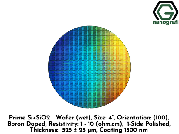
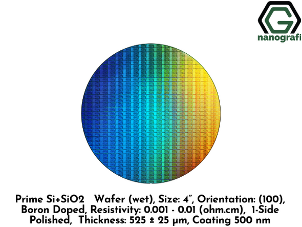
Description
1 piece/75 €
5 pieces/252 €
25 pieces/1068 €
Please contact us for quotes on larger quantities !!!
Prime Si+SiO2 Wafer (wet)
Size: 4”, Orientation: (100), Boron Doped, 1-Side Polished, Thickness: 525 ± 25 μm, Coating 300 nm
Technical Properties:
|
Quality |
Prime |
|
Materials |
Si + SiO2 (wet) |
|
Size (inch) |
4” |
|
Orientation |
(100) |
|
Coating |
300 nm |
|
Thickness (μm) |
525 ± 25 |
|
Doping |
Boron |
|
Resistivity (ohm.cm) |
1-10 |
|
Polished |
One Side |
Silicon dioxide wafer – also referred as thermal oxide wafer- is produced at elevated temperatures.
Thermal oxide is normally grown in a horizontal tube furnace, at temperature range from 900°C ~ 1200°C.
Thermal oxide is a kind of "grown" oxide layer , compared to CVD deposited oxide layer , it has a higher uniformity, and higher dielectric strength , it is an excellent dielectric layer as an insulator.
In most silicon-based devices, thermal oxide layer plays an important role to pacify the silicon surface to act as doping barriers and as surface dielectrics.
It allows a very good thickness uniformity and purity.
Therefore, this is the preferred way to produce high quality thin silicon oxide layers.
Thicker oxide layers are typically produced by wet oxidation where the growth rate is significantly increased.


