Description
1 piece/162 €
5 pieces/763 €
25 pieces/3108 €
Please contact us for quotes on larger quantities !!!
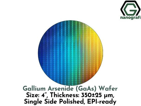
Gallium Arsenide (GaAs) Wafer
Size: 2”, Thickness: 350±25 μm, Single Side Polished
Technical Properties:
|
Quality |
GaAs |
|
Materials |
GaAs |
|
Size (inch) |
2” |
|
Thickness (μm) |
350± 25 |
|
Polished |
Single Side |
|
Dopant |
Silicon ( N type ) |
|
Orientation |
(100)15 deg off toward <111>A±0.5 |
|
Resistivity |
(1.2—9.9) E-3 |
|
Mobility |
1000-3000 |
|
EPD |
≤3000 |
|
Growth method |
VGF |
|
OF Length |
17±1 |
|
IF Length |
7±1 |
Fields of Application for Gallium Arsenide (GaAs)
Gallium arsenide (GaAs) is a compound of the elements gallium and arsenic.
Gallium arsenide (GaAs) is a semiconductor compound. Gallium arsenide (GaAs) has a high electron velocity and high saturated electron mobility.
This makes gallium arsenide (GaAs) components are useful in fast electronic switching applications and at ultra-high radio frequencies.
In 1907, the British discovered infrared emmission from gallium arsenide. This was called electroluminescence. Also, gallium arsenide (GaAs) was
used as a solar cells in space for the Venera 3 mission in 1965, which is the first known operational use of gallium arsenide (GaAs).
Vertical gradient freeze is the most common method to produce GaAs wafers.
Mainly used for circuits, electronics and solar cell applications.
Carbon, silicon, tellurium and zinc are some of the dopants that are used to modify the characteristics and electrical properties of gallium arsenide wafers.
Wafer flatness and surface purity are ensured by highest quality standards.
Boron concentration of gallium arsenide wafers highly depend on the production method.
Gallium arsenide wafers with adequate electrical resistancy prevent high current induction in the circuit.
Mobility of GaAs wafers can be tailored with different doping levels.
- Gallium arsenide (GaAs) is used in laser diodes.
- Gallium arsenide (GaAs) is used in solar cells.
- Gallium arsenide (GaAs) is used in optical windows.
- Gallium arsenide (GaAs) is used in monolithic microwave integrated circuits.
- Gallium arsenide (GaAs) is used in microwave frequency integrated circuits.
- Gallium arsenide (GaAs) is used in infrared light-emitting diodes.
- Gallium arsenide (GaAs) is useful in barometers.
- Gallium arsenide (GaAs) is useful in pharmaceuticals and nuclear medicine tests.
- Gallium arsenide (GaAs) is useful in high temperature thermometers.


