
What is Graphene: The Ultimate Guide
Explore graphene's groundbreaking journey, from discovery to revolutionary applications across diverse fields.
Key Takeaways
- Graphene is a revolutionary, atom-thick carbon material with exceptional strength and conductivity.
- Its discovery and applications span from electronics to medicine.
- Graphene's production and future potential are evolving.
In fact, in our ultimate guide to graphene, we'll shed a light on the matters such as production of graphene, and how a single layer of carbon atoms may be stronger than anything. Continue reading to learn more.
Table of Contents
- Introduction: What is Graphene?
- Part 1: History of Graphene
- Part 2: Properties of Graphene
- Part 3: Applications of Graphene
- Part 4: Graphene Production
- Part 5: Popular Graphene Products & Solutions
What is Graphene?
Graphene is a layer conductor of carbon atoms arranged in a hexagonal lattice, just one atom thick. This unique structure makes it one of the thinnest, strongest, and most conductive materials known. Because of its superior properties, graphene is used in a wide range of fields from electronics to energy storage systems, from medicine to material science, and has a vast potential for applications.
Graphene is formed by stacking layers of graphite on top of each other. While graphite is a natural substance found in many products from pencils to batteries, graphene obtained by separating these layers has extraordinary physical and chemical properties. Isolating a single layer of graphite makes the discovery of this incredible material, namely graphene, possible.

Structure of Graphene
The graphene is an allotrope of carbon, that is, a form in which carbon occurs. Other allotropic forms of carbon are graphite or diamond.
Graphene is formed by hexagonal rings of carbon atoms, one of the most important and abundant elements in nature. Each layer of hexagonal graphene ring has a height of approximately one carbon atom and this characteristic, together with the application of very specialized techniques, allows us to obtain extraordinarily thin graphene layers.
The perfect graphene would contain only hexagonal rings although, in reality, pentagonal and heptagonal rings may appear that are considered irregularities and imperfections in the structure of graphene. This structure is the basis of other graphite substances such as fullerenes, carbon nanotubes or graphite itself.
Graphene is the basic elementary unit in 2D to build all the graphite materials of other dimensions. For example, it can be arched in zero-dimensional structures (0D), as is the case with fullerenes, it can be rolled up in 1D structures, giving rise to carbon nanotubes and, finally, it can be stacked successively giving rise to three-dimensional graphite (3D).
According to the IUPAC (International Union of Pure and Applied Chemistry), the term graphene should be used when talking about "reactions, structural relationships or other properties of individual layers" of carbon. Taking this into account, it is not correct to describe graphene as "layers of graphite" (graphite implies 3 dimensions while graphene implies carbon bonds in two directions), "carbon sheets" and similar concepts. Thus graphene can be defined as an infinitely alternating polycyclic aromatic hydrocarbon of six carbon atoms rings, that is, it a flat molecule composed of carbon atoms that form a pattern of hexagonal rings.

Figure 1. Graphene Structure
Part 1: History of Graphene
The 21st century, after the eras of coal and silicon, has been defined as the era of Graphene, considering that graphite, the allotrope of carbon from which Graphene originates, is a poor and abundant material in nature so it can be exploited on an industrial level. The carbon atom is one of the most intriguing elements of the entire periodic table, a brick on which the entire system of organic chemistry is built and above all constitutes the fundamental element of Graphene.
But where does the story begin? Very far away, even from the Middle Ages when graphite was used as a marking tool. In practice, when we rub a graphite sample on a sheet or on another support, very thin layers of material adhere to the support and then remain there. Around 1560, Bernacotti gave the idea of a lead pencil. In 1795, its production on a large scale came into existence. It is logical to think that an object as humble as a pencil may have contributed, in some way, to increase the ability to acquire culture even on the part of the less advantaged social strata that rarely could afford the luxury of buying books.
The history of Graphene is long and peculiar from many points of view, it is curious and partly surprising to see how. Despite the fact that graphite was in our hands for centuries, Graphene was never actually recognized as a material destined to change the entire history of science; this lack of recognition was probably due to the lack of adequate investigation tools. Now we can, with good reason, state that this innovative field of research is the most explored in the world, not only from an experimental point of view but also from a theoretical point of view.
The first work on the band structure of the single graphite plane date back to a period between 1947 and 1958, a time when, however, this material was considered only an academic exercise, because the same researchers believed that it was impossible to obtain strictly two-dimensional system that is simultaneously stable even in the isolated state. Boehm and his colleagues, in 1986, coined the term " graphene" combining the word graphite and a suffix that refers to a particular type of hydrocarbons, i.e. polycyclic aromatic hydrocarbons. In 1999, the first free graphite was built and only 5 years later, the history of science changed completely.
In 2004, at the University of Manchester, the scientists Geim and Novoselov, using a graphite sample and a simple adhesive tape discovered the material of the future that is Graphene. From a structural point of view, we can imagine Graphite as a book whose sheets are made of Graphene.
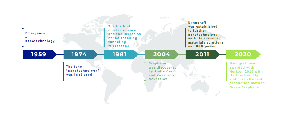
Figure 2. Nanografi's Graphene & Nanotechnology Journey
Discovery of Graphene
The discovery of Graphene is quite recent and, perhaps, for this reason, it is a material still unknown to a large number of people. It was first obtained in 2004 when two professors from the University of Manchester (United Kingdom) had the unusual idea of using adhesive tape (the common Scotch tape) to skin a piece of graphite. Thus they created the first Graphene in history.
This new material, considered the "wonder material" of the 21 st century, is a crystalline allotrope of carbon, a characteristic it shares with diamonds and graphite. All three are made up of carbon atoms joined together in different ways. For example, graphite consists of carbon atoms bonded together in layers of a hexagonal lattice, while Graphene is made up of a single layer of graphite. It might seem like a laboratory curiosity for chemistry enthusiasts. In fact, the potential commercial applications and profit opportunities of Graphene are so great as to overcome even the most fervent imagination. That's why we've put together this brief overview of Graphene, its production, its applications and what it could give us in the future. More than 200 companies and start-ups are involved in research around Graphene. In 2010, it was the subject of nearly 3,000 research papers.
Who Discovered Graphene?
In 2004, at the University of Manchester, Andre Geim and Konstantin Novoselov successfully isolated graphene, which is a single carbon atom layer from graphite. This revolutionary discovery introduced the material's unique and superior properties to the world. This groundbreaking discovery has awarded the duo the Nobel Prize in Physics in 2010.
Andre Geim, a Dutch citizen, was born in 1958 in Sochi, Russia, where he graduated in 1987, at the Institute of Solid State Physics in Chernogolovka. He is currently head of the University of Manchester Center for meso-science and nanotechnology. Geim was also the winner in 2000 of IgNobel, the prize awarded to the "most unlikely" research, for having used magnetic fields to levitate a frog, assisted in this task by Sir Michael Berry, of the University of Bristol, known for his research in the quantum field. For "Le Scienze", Andre Geim illustrated his research in an article, written in collaboration with Kim Philip and published in June 2008.
On the other hand, Konstantin Novoselov has dual citizenship, Russian and British. He was born in 1974 in Nizhny Tagil, Russia. He then specialized at Radboud University in Nijmegen, the Netherlands. He is currently working at the University of Manchester.
Understanding Graphene
Before talking about graphene’s structure and properties in detail, let's try to understand graphene as a non-scientist.
Graphene is considered one of the great revolutions of the 21 st century if we talk about new materials. Graphene is so tough that a cat could swing in a graphene hammock, which would weigh less than one of its whiskers. Also, this would be virtually invisible. Discovered in 2004 by Andrei Geim and Konstantin Novoselov, Graphene has millions of applications to the real world that will arrive in the coming years.
Graphene is about 200 times stronger than steel and 1000 times lighter than a sheet of paper. The enthusiasm for graphene has been totally unexpected and no one imagined that a sheet of this material could be so thin, such a good conductor of electricity, and so resistant. It is even expected that new qualities will be discovered over time.
Graphene is still in the laboratories and there are companies that manufacture and sell graphene. Large companies are already working with this material, as is the case of Toshiba, which would be using it to cover the cables that we found inside their computers.
Graphene has a plethora of applications in our daily lives. It has flexible touch screens, sensors, and fast data transmission devices by optoelectronics. In China, there is a flexible screen prototype made of graphene and the aviation companies Airbus and Boeing are interested in this material to reinforce the structures of their aircraft.
With treatment, you can get it to only transmit electricity in one direction. Moreover, Graphene has really interesting biological & medical applications, such as a graphene structure to grow artificial organs with stem cells.
Part 2: Properties of Graphene
The features of Graphene are extraordinary. Graphene is a substance with very interesting characteristics, some amazing. These properties together with the abundance of carbon in nature have made graphene earn the name of "material of the future." Some of the most outstanding features of graphene are high thermal conductivity, high electrical conductivity, high elasticity (deformable), high hardness (resistance to being scratched), and high resistance. Graphene is approximately 200 times stronger than steel, similar to diamond resistance, but is much lighter.
Moreover, Graphene is more flexible than carbon fiber but just as light. The ionizing radiation of Graphene does not affect you. Graphene has a low Joule effect (heating when conducting electrons). For the same task, graphene consumes less electricity than silicon. Graphene is capable of generating electricity by exposure to sunlight. Graphene is a virtually transparent material. Graphene is very dense and does not allow helium to pass in gaseous form, however, if it is allowed to enter the water, which, enclosed in a graphene container, it shows an evaporation rate similar to that shown in an open container.
We can’t stop praising the properties of Graphene. Other features still under discussion are the self-cooling capacity described by researchers at the University of Illinois or its ability to self-repair. If a layer of graphene loses some carbon atoms for any reason, the atoms close to the hole left approach and close the hole, this capacity for self-repair could increase the longevity of graphene-manufactured materials, although in a limited way.
Key Points:
- Extreme Strength
- Superior Electrical Conductivity
- Exceptional Thermal Conductivity
- Single-Atom Thickness
- High Flexibility
- Lightweight Nature
- Transparency
- Chemical Stability
- Large Surface Area
- Biocompatibility
Why Graphene is Important?
Graphene is so important and said to be the "miraculous material" of the 21 st century and its properties have astonished science and the media. Most of the applications proposed for graphene are electronics and computer science. Its electronic features can be used for the manufacture of transistors for high-speed electrical circuits and could ultimately replace silicon in microchips and forever change the future of computers and other devices.
Good graphite is not easy to find and its prices have doubled in recent years. A ton of graphite with a purity of 97% costs about 2,000 dollars. A ton of 99.99% ultrapure graphite costs 20,000. Graphene can be used for anything from composite materials such as carbon fiber today, to electronics. The ways in which graphene can be used are as surprising as their properties. Graphene does not have only one application, it is not even a unique material. Graphene is 'a huge variety of materials'.
The benefits of using graphene for businesses and consumers would be obvious, the devices would be faster and cheaper as well as thinner and more flexible." Theoretically, you could roll up an iPhone and stick it behind your ear like a pencil," Professor James Tour of Rice University told Technology Review magazine.
If graphene is compared with the way plastic is used these days, in the future credit cards could have the same processing power as a current smartphone. "A completely new world of electronic applications can be opened with the transparency, flexibility, and speed of graphene," says Jari Kinaret, Professor of Technology at the Swedish University of Chalmers. In Europe, graphene research will receive an investment of one billion euros from the European Commission in the next 10 years.
The multinational Samsung in collaboration with the Sungkyunkwan University of South Korea is one of the largest investors in graphene research and has developed a 25-inch flexible touch screen with graphene. Companies like IBM are also investigating. IBM has created a 150 gigahertz (GHz) transistor. The fastest comparable silicon device is around 40 GHz. With all the money invested and market expectation, scientists are cautious about how quickly all this potential can come true.
Flexibility & Strength of Graphene
Despite being incredibly thin, graphene is flexible and robust, which opens doors to applications in wearables and aerospace technology.
It is the strongest material known to science, with a tensile strength of up to 130 gigapascals (GPa), which is about 200 times stronger than steel. Graphene is also incredibly flexible, able to stretch up to 20% of its original length without breaking.
The flexibility of graphene is due to its unique molecular structure. The carbon atoms in graphene are bonded together in a hexagonal lattice, which gives the material its strength and stiffness. However, the bonds between the carbon atoms are also relatively weak, which allows the material to bend and deform without breaking.
The strength of graphene is due to the strong covalent bonds between the carbon atoms. These bonds are very difficult to break, which gives graphene its incredible tensile strength. In fact, graphene is so strong that it is considered to be one of the strongest materials in the universe.
Graphene's flexibility, strength, and versatility hold promise for applications ranging from lightweight aerospace materials to innovative sensors, batteries, medical devices, and barrier-based solutions such as flexible electronics, bulletproof armor, sports equipment, medical implants, packaging, and water purification.
Graphene is the material with the highest mechanical strength of all materials known in nature, it is even much stronger than the strongest of steels. This property makes graphene a material that can be very useful in applications where high mechanical strength and low weight are required. The extraordinary strength of graphene gives rise to a lot of applications in different sectors.

Figure 3. Strenght of Graphene
Mechanical Resistance of Graphene
The origin of the great mechanical resistance offered by graphene must be found in covalent bonds type σ that is established between the carbon atoms that make up its crystalline network. The main mechanical properties of a material, such as its breaking stress, its rigidity, fragility, resilience or toughness can be deduced from the stress-strain curve obtained from the tensile test of a sample of material.
As is known, this test consists of subjecting a cylindrical specimen of material to a certain mechanical tension (σ) (force per unit area) in the longitudinal direction to its main axis, until its breakage occurs, then measuring the deformation that originates (ε) in the specimen.
The mechanical resistance values in conventional materials (macroscopic) refer to the force necessary for the breaking of a sample of the material with a given section, and therefore, its units are measured in N/m 2 (Newton/meter2). But such tests cannot be carried out to determine the mechanical properties of materials that are formed in the form of microscopic membranes, such as Graphene.
Graphene is the Strongest, Hardest & Lightest Material
Graphene is the strongest, hardest, and lightest of the materials ever made. In its version with 2 dimensions, graphene is the strongest of materials. However, until now researchers have had difficulty translating this two-dimensional force into a useful three-dimensional material. These two-dimensional materials have exceptional strength and unique electrical properties.
The researchers were able to compress small graphene flakes using a mixture of heat and pressure. This process has produced a very strong and stable structure, whose shape resembles that of some corals. These forms, which have an enormous surface in proportion to their volume, have proven to be extraordinarily strong. Once these 3D structures were created, the researchers then wanted to see how far they were able to push themselves by designing the strongest material that could be produced. To do this, they created a variety of 3D models and subjected them to various tests. One of the samples showed 5% of the density of the steel and 10 times its strength.
The new results show that robustness is not only a characteristic of two-dimensional materials similar to graphene but also depends on the geometric structure. This suggests that other materials, strong and light like graphene, could be made more resistant with a three-dimensional structure.
How Strong is Graphene Compared to Other Materials?
When talking about the strongest materials, we can find many competitors of Graphene. Let’s discuss the top ten strongest materials in the world.
Diamond is a ceramic material of natural origin made of carbon atoms tightly bonded together in a network. Diamonds are almost impossible to scratch.
On the other hand, Spider Silk has a very high tensile strength. A silk thread can withstand more pull before breaking than steel.
When talking about Carbon, there are many different types of carbon composite materials but they all exhibit great strength properties. They can resist an immense amount of tension and absorb a great deal of force before breaking.
Osmium is another metal which is the strongest element of the platinum family. When it is isolated, osmium is a very hard and extremely dense silver metal.
Moving on, martensitic steels have strength and resistance superior to normal steel but without losing the malleability. Moreover, metallic crystal has a chemical structure that counteracts the inherent fragility of glass but maintains its resistance. It is not very dense and is lighter than steel.
Wurtzite Boron Nitride is very similar to a diamond on a structural level, but 18% harder. While diamonds are produced from carbon under pressure, Wurtzite Boron Nitride (WBN) is born from the heat and pressure produced during volcanic eruptions.
The next strongest element is Lonsdaleíta. With this difficult name, it is known what is possibly the hardest material of natural origin. It is similar to diamond, but 58% harder. Sometimes it forms when meteorites that contain graphite hit the Earth.
In the end, the king of the strongest materials is Graphene. Graphene consists of a single atomic layer of carbon, organized in a honeycomb structure. In its perfect crystalline form, graphene is the strongest material ever measured.
Conductivity of Graphene
Conductivity can be defined as the quality of being able to transfer sound, electric charge or heat. It can also be defined in terms of density, electron mobility, temperature, and other important parameters.
Electrical conductivity refers to charging mobility in an electric field, which increases as the temperature drops. Graphene is a very good conductor of heat and electricity. Observing the unusual movement of electrons in graphene, researchers at the University of Manchester have discovered a new understanding of the conductivity physics of materials.
The experiments performed have provided an essential understanding of the peculiar behavior of the flow of electrons in graphene, discovering a set of properties that must be taken into account for the design of future nanoelectronics circuits.
Graphene is widely a better conductor than copper, thanks in large part to its two-dimensional structure. In most metals, conductivity is limited by crystalline imperfections, which cause electrons to disperse like billiard balls when they move through the material.
Electrical Conductivity of Graphene
Graphene exhibits incredibly high electrical conductivity surpassing even copper. This makes it a top contender for future electronic devices.
Graphene's high electrical conductivity is due to its unique electronic structure. Graphene is a semimetal, which means that it has both metallic and insulating properties. The metallic properties of graphene are due to the presence of delocalized electrons in the graphene sheet. These delocalized electrons are free to move throughout the graphene sheet, which allows for the rapid conduction of electricity.
The electrical conductivity of graphene can be affected by a number of factors, including the purity of the graphene, the presence of defects, and the environment in which the graphene is used. However, even with these factors taken into account, graphene remains one of the most conductive materials known to man.
Graphene's high electrical conductivity has a number of potential applications in electronics, energy storage, and other fields. For example, graphene could be used to make transistors that are much smaller and faster than current transistors. Graphene could also be used to make flexible electronic devices and sensors.
Thermal Conductivity of Graphene
Graphene exhibits a remarkably high thermal conductivity. This unique characteristic holds the potential to revolutionize the field of thermal insulation materials.
Thermal conductivity is the ability of a material to transfer heat from one part to another. It is measured in watts per meter per Kelvin (W/m/K). Graphene has a thermal conductivity of up to 5000 W/m/K at room temperature, which is much higher than most other materials.
There are two main reasons for graphene's high thermal conductivity. First, graphene has a very strong covalent bonding structure. This allows heat to be transferred efficiently between the carbon atoms. Second, graphene has a very low phonon scattering rate. This means that phonons, which are the quantum of heat, can travel long distances without colliding with defects or impurities.
Graphene's high thermal conductivity has a number of potential applications. For example, it could be used to develop new thermal management materials for electronic devices. Graphene could also be used to create new types of heat sinks and thermal interface materials.
In addition, graphene's high thermal conductivity could be used to develop new types of sensors and actuators. For example, graphene could be used to create sensors that can detect temperature changes very quickly. Graphene could also be used to create actuators that can be used to control heat flow.
Researchers are still working to understand the fundamental mechanisms behind graphene's high thermal conductivity. However, the potential applications of graphene's thermal properties are vast.
Graphene holds potential for enhanced thermal management in electronics, offering improved materials for heat sinks, thermal interfaces, and novel sensors and actuators for heat flow detection and control across multiple industries.
Transparency
Comparable to glass in transparency, graphene has potential in the development of transparent electronics.
A single sheet of graphene absorbs only about 2.3% of visible light. This means that graphene is nearly transparent to visible light, with a transparency of around 97.7%. This is even more transparent than many other transparent materials, such as glass (around 90% transparent) and plastic (around 92% transparent).
Graphene's transparency is due to its unique electronic structure. Graphene is a zero-bandgap semiconductor, which means that its electrons can move freely throughout the material. This allows graphene to absorb very little light, even at visible wavelengths.
However, the transparency of graphene can be affected by a number of factors, including the thickness of the graphene film, the presence of defects in the graphene film, and the wavelength of light. For example, thicker graphene films are less transparent than thinner graphene films. Additionally, graphene films with defects will absorb more light than graphene films without defects. Finally, graphene is more transparent to longer wavelengths of light than to shorter wavelengths of light.
Despite these factors, graphene has the potential to be used in a wide range of applications that require transparent conductors. For example, graphene could be used to make transparent electrodes for solar cells, touch screens, and other electronic devices. Graphene could also be used to make transparent conductive coatings for windows and other glass surfaces.
Researchers are currently working to develop methods for producing high-quality graphene films with high transparency. As these methods are developed, graphene is expected to play an increasingly important role in a variety of transparent electronic devices.
Graphene can revolutionize transparency in technology by offering efficient electrodes for solar cells, more responsive touch screens, conductive window coatings for energy and temperature control, and thinner, energy-efficient displays.
Graphene Benchmark in Material Science
Graphene vs. Diamond
Diamond consists of pure crystallized carbon and it is very hard. It has an index of 10 on the scale of Mohs hardness (the scale ranges from 1 - 10). The diamond word etymologically means unchanged, which is not new given its very high hardness. While talking about its physical properties, they are among the best of all the stones used to make jewelry.
Diamond consists of carbon, it is the precious stone whose composition is the simplest, other precious stones are all complicated. The diamond sometimes has traces of nitrogen that can go up to 0.20% and a very small proportion of other elements. The diamond crystal would have formed by repetition and stacking in the 3 directions of the space of carbon atoms that could be compared with cubic tetrahedra whose center would concentrate the mass of the atom and in which the 4 vertices would have an electron. Each atom is linked, hooked to others by very strong and very short bonds.
These bonds are covalent, and each center of these atoms is distanced from its neighbor only by a distance of the order of 1.54 angstrom, that is, 0.000.000.154 mm. Since the atomic bonds of the diamond are very short, this partly explains its great hardness.
Graphene, which is also composed of carbon, is a soft mineral. Unlike the diamond, their atoms are quite far from each other. If you compare these two minerals (diamond and graphene), which are both carbon compounds, the result is surprising: one (the graphene) is stronger as compared to a diamond and it is 200 times stronger than steel. So, we can say that Graphene is stronger than diamond.
Graphene vs. Graphite
Graphene is one of the finest materials in the world, it has only two dimensions and has a thickness of a single atom. It is a layer of graphite, discovered thanks to the pencil lead and scotch rolls. The ductility, strength, elasticity and conductivity make it suitable for making significant scientific innovations. Graphene derives from graphite, the mine of our pencils: it is a two-dimensional material, consisting of a single layer of carbon atoms, placed at the vertices of regular hexagons that follow one another on a planar lattice. It has interesting properties that make it a promising candidate for numerous applications.
On the other hand, graphite is a mineral of elementary class, and its specific composition involves a semi metallic element.
Surely you are interested to know what graphite is made of. The composition consists almost exclusively of carbon atoms, and it is, in fact, one of the allotropic forms in which elemental carbon can be presented, together with diamond, fullerene, and others, such as graphene.
It is the most stable form of carbon in standard conditions (or at low pressures and temperatures), so it is used in thermochemistry to define the standard state in which the heat of formation of carbon compounds is measured.
The chemical formula of Graphite is C. It is also polymorph of the chaoïta and the lonsdaleïta. This term has its origin from the Greek γραφειν (graphein) which means to write. The composition of graphite can be considered as the maximum carbon content, being above anthracite, so it can be called meta-anthracite, although it is not normally used as fuel because it is very difficult to ignite it. It is also possible to understand this mineral as a succession of overlapping graphene layers. Thus, we can say that graphene is just a layer of graphite.
Graphene vs. Steel
Steel is an alloy (combination or mixture) of iron (Fe) and carbon (C) provided that the percentage of carbon is less than 2%. This percentage of carbon usually varies between 0.05% and 2% maximum. Other materials such as Cr (Chromium), Ni (Nickel) or Mn (Manganese) are sometimes incorporated into the alloy in order to achieve certain properties and are called alloy steels.
On the other hand, graphene is 200 times stronger than steel. Graphene is a layer of graphite, the carbon crystal with which pencil mines are made. Its extraordinary properties were known in the 40s of the 20th century, but it had not been possible to obtain it. It was only in 2004 that scientists from the University of Manchester succeeded. They were able to "peel" graphite layer by layer and separate the graphene. Of course, they won the Nobel Prize. Why? For those extraordinary properties, study Features of Graphene above. And, based on them, new applications are being investigated. For example, clothes with special thermal capacities, a completely new electronics, faster and more efficient than the current one based on silico published a study, in the automotive and aeronautical industry due to its hardness, generation of living tissue, among many more.
Graphene vs. Carbyne
Carbyne is approximately twice as strong as graphene and carbon nanotubes, which until now were the most resistant materials. Researchers at Rice University on the properties of carbyne, material that has proven to be stronger than graphene. It also has remarkable electrical properties.
Nowadays it is manufactured in small quantities, so the manufacturing process would have to be greatly improved to make it viable. Carbyne is a structure that consists of carbon atoms joined in double sequential bonds, or alternated between single and triple bonds.
Like graphene, the structure has a single atom of thickness and has the peculiarity of being very flexible, but not stretchable. The researchers also showed that when the carbyne is bent in an arc or circle, the tension between the atoms can alter the so-called banned band. This property could open the doors to a lot of mechanical and electronic uses.
After comparing Graphene with other components, and knowing about its strength, what graphene can do for our protection?
Graphene vs. Bullet
Graphene is a paragon of promises. It is known as the material of the future, one of the thinnest, flexible and strongest in the world, which could revolutionize our world with multiple applications in the mobile phone, telecommunications, chip manufacturing or medical equipment industry. But it is also that this wonderful material could become a harder armor than steel and kevlar, capable of resisting a bullet like a real "terminator."
Graphene is characterized by having a single layer of carbon atoms arranged in a hexagonal lattice, it has proven to be the strongest material of the world, measuring the resistance of the sheet being pressed with a diamond tip. But now, the material has proven to be bulletproof, research published in the journal Science.
A team from the University of Massachusetts at Amherst fired tiny spheres of silica in the graphene layers as if it were a micro camping range. The bullets flew at a speed of 6,700 mph, about a third of the speed of a real bullet. The result was shocking. Graphene sheets absorbed the impact twice as well as Kevlar, the most commonly used material in bulletproof vests, and tens of times better than steel.
This opens the door to a new use for graphene. Because it is so thin, light and strong, it could be used to make defensive suits and vests for security forces or military personnel. Now, the key is to achieve that graphene can be manufactured on a large scale without modifying its wonderful characteristics. A good number of companies are chasing it.

After comparing graphene and other materials, learn how to identify fake graphene.
Part 3: Applications of Graphene
It has been known for a long time that graphene is the material of the future. More precisely, since 2010, when the Nobel Prize for Physics was awarded to two Russian researchers, Kostya Novoselov and Andre Geim, who, some years before, had succeeded in isolating the thinnest material in the world with the sole aid of a 2-pound scotch roll. Since then, research projects on the material and its possible applications have multiplied all over the world, involving the EU itself, which has earmarked 1 billion euros in the largest European initiative on the subject, Graphene Flagship.
The properties of graphene make it an ideal material for applications in a variety of sectors. For example, graphene can be used in technology, especially in electronics in the manufacturing of integrated circuits. It is assumed that graphene characteristics can make it possible to build processors much faster than current ones.
This speed has already been put into practice in the manufacture of field-effect transistors built with graphene. These transistors also take advantage of the high mobility of carriers with low noise levels presented by graphene.
Among the potential applications of graphene can be cited as the most interesting:
- Ethanol Distillation: Room temperature distillation for fuel and consumption.
- Gas Detection: Ultrasensitive graphene-based gas detectors.
- Optical Modulators: Enhancing light manipulation.
- Solar Cells: Efficient energy conversion.
- Graphene Transistors: Pioneering faster electronics.
- Integrated Circuits: Enhanced speed and efficiency.
- Electrochromic Devices: Advanced light modulation.
- Ultra-Fast Battery Charging: Revolutionizing power storage.
- Transparent Electrodes: For innovative electronic displays.
- Antibacterial Applications: Novel healthcare solutions.
- Radioactive Waste Collection: Streamlining decontamination processes.
- Sports Equipment: Stronger, balanced tools and gear.
- Ultra-Thin Touchscreens: Flexible, durable displays.
- Supercapacitors: Potentially replacing traditional batteries.
- Flash Memory: Faster data storage solutions.
- Biosensors: Quick, efficient health monitoring.
- E-Paper: Updateable and reusable digital paper.
- Audio Technology: Headphones with exceptional sound quality.
- Aerospace and Armor: Enhanced strength and weight efficiency.
- Waterproof Coatings: New levels of protection.
- Bionic Devices: Direct neural integration.
- Folding Batteries: Innovative energy designs.
- Tissue Regeneration: Advancements in medical technology.
- Water Purification: Transforming saltwater into drinking water.

Explore the diverse uses and applications of graphene for further insights.
Graphene's Applications and Real-World Use Cases
Graphene in Composites and Coatings
Graphene is a very thin material, but it has great strength which enhances the mechanical strength of the polymer with high thermal and electrical conductivity such as, 15-50 percent increase in mechanical strength is possible by adding a particular quantity of graphene in nylon 66. When graphene is added in silicone rubber, the tensile strength is enhanced by 2 times for the support component. If graphene is added in nitrile-butadiene rubber, its mechanical properties is enhanced by 1 - 5 times. Also in another normal high polymer like PP, PVC, and resin, the properties of graphene are improved greatly. Graphene's superior properties make it a better material than other coatings in many ways.
Use Case: Graphene 3D's New G6-Impact Composites
The American Graphene 3D Lab has announced the development of a new family of composite materials based on a matrix of crystal polystyrene (HIPS) reinforced with carbon fibers and particles. The products will be marketed under the G6-Impact brand both in the form of a filament for 3D printing and in granules for injection molding. The company produces the materials at its New York facility and is already able to supply limited quantities of application development material.
The performance of these carbon-graphene composites promises to be very high. According to the company, the material offers excellent rigidity combined with extraordinary shock and vibration absorption properties, thanks to both the patent formulation and the production process. The new composites would be suitable for applications requiring high resilience, shock absorption and vibration damping on hard surfaces such as sports equipment, robots, power tool handles car components, drones and parts of airplanes or military equipment.
Graphene in Electronics
Graphene is a material that can revolutionize the composition of electronic devices that we know today. Graphene is so important for every electronic device we use every day.
Thanks to its high electrical and thermal conductivity, Graphene can be widely used in electronics. For example, Transistors, microprocessors and integrated circuits benefit from the mobility of electrons which is particularly high in graphene.
Also for the storage of energy, there may be good developments. The batteries based on graphene, for tablets and other mobile devices, provide performance superior to those current and smaller dimensions because, thanks to its nanometric dimensions, this material can accumulate more energy in smaller spaces.
Use Case: NTNU's Graphene Semiconductors
Semiconductors developed from graphene can change the technology industry in five years. Researchers from the Norwegian University of Science and Technology (NTNU) have developed - and patented - a hybrid material with very interesting properties. These are gallium arsenide nanotubes (GaAs) developed on graphene, which is a layer of highly alloyed carbon atoms arranged in hexagonal order.
According to Professor Helge Weman of NTNU, "The new hybrid material offers excellent optoelectronic properties". He is also the co-founder of CrayoNanoAs, the company created to commercialize the discovery.
The growth of nanowires on graphene occurs with a method called MBE (Molecular Beam Epitaxy). It is a model for a new method of manufacturing semiconductor devices. Among the first future applications, we see solar cells and light-emitting diodes (LEDs).
Companies like IBM and Samsung are leading the development of graphene to replace silicon in electronics and create new applications, such as flexible touchscreens for smartphones. They no longer have to wait. This invention fits perfectly into their production machinery and allows consumer electronics to be brought to a level where design has no limits.
According to the researchers, thanks to this invention in the future we could have self-powered nanomachines and advanced 3D integrated circuits made on graphene and nanowire semiconductors, which allow us to create smaller and more efficient electronics. Furthermore, there is also a discussion of flexible and self-powered consumer electronics to be included in clothes, notepads and other devices, such as smartphones and tablets. Professor Weman highlights that the semiconductors developed on graphene could become the basis of new types of systems and transform the semiconductor industry using graphene as a preferred substrate for many applications.
Graphene in Electrodes
The use of graphene electrodes could lead to the creation of new energy storage devices suitable for electric vehicles, renewable sources and smart grid applications.
In an article published in the prestigious magazine Nano Letters, researchers from two US companies proposed a new technological solution capable of combining the advantages of electrochemical batteries with those of double-layer capacitors (supercapacitors), so to obtain energy storage systems with high power combined with high energy density.
All the scenarios of the possible development of sustainable mobility and energy supply are closely related to the construction of suitable energy storage devices. Currently, the most promising devices are supercapacitors and lithium batteries.
Both solutions have some disadvantages: while lithium batteries offer high energy density with low power density, supercapacitors, on the contrary, can provide high power density, but with low energy density. Supercapacitors, unlike conventional condensers, are not based on the use of a dielectric material. The electrolyte of the condenser, due to the "double layer" electrical effect, leads to effective charge separation, even if the physical separation of the layers is imperceptible.
In general, supercapacitors offer advantages such as high power density, long life, simple recharging circuits, high safety, and low costs. However, they also have some disadvantages, such as a low amount of energy stored per unit of weight, a high self-discharge and a maximum achievable low voltage.
The lithium-ion battery, on the other hand, can generally be described by three main functional components, namely the anode, the cathode and the electrolyte. The non-aqueous electrolyte is commonly made up of a mixture of organic carbonates and contains lithium ions. The cathode is based on metal oxide and the most common material for the anode is graphite. These batteries have the diffusion of lithium ions between the anode and the cathode, with the possibility of these ions to migrate to or from the anode and the cathode. However, the low solid-surface diffusion limits the maximum power density. To date, there is a strong research activity for the improvement of each of these individual devices, but new approaches to the problem are also being investigated.
Use Case: Supercharging Batteries with Graphene Technology
Recently research activities have focused on how to apply nanotechnologies in order to increase the characteristic power density of lithium-ion batteries. In the research presented by Nanotek Instruments and Angstron Materials, the researchers chose a new approach, using nanostructured graphene as electrode material. In prototype devices made during the research, the nanostructured porous graphene is connected both to the anode and to the cathode, in two distinct blocks separated by a porous membrane, and is immersed in the electrolyte. The current flow is based on the exchange of lithium between the surface of the two nanostructured graphene electrodes. The two graphene surfaces can capture lithium ions quickly and reversibly, through surface adsorption mechanisms and/or surface redox reactions.
The authors of the research carried out experiments using different graphene structures. The study is still in a preliminary phase, but results have been so promising that the hypothesis of a future realization of systems able to reach energy densities of 160 Wh/kg per cell unit is possible. This value is over 30 times higher than that achievable with conventional supercapacitors and is comparable with that of lithium-ion batteries. In addition, these systems can reach power densities of 100 kW/kg per cell unit, 10 times higher than those of traditional supercapacitors and even 100 times greater than lithium-ion batteries.
Graphene in LCD and LED Monitors
Graphene is one of the hopes for the achievement of flexible technology. Although today some designs have been achieved based on traditional materials used in electronics, including some timid commercial appearances, the compound that won the Nobel Prize in Physics to Andrey Geim and Konstantin Novoselov promises much more than it has been until now. Another proof of the possibilities of the material are the prototypes of graphene-based LED screens that have been built in the laboratory.
Use Case: Graphene-Driven LED Screens for Next-Gen Electronics
Researchers at the University of Manchester and the University of Sheffield have worked together to develop a semi-transparent device composed of graphene-based LEDs, whose characteristics could be the basis of a future generation of mobile phones, tablets or flexible televisions.
The product resulting from the research is an extremely thin semiconductor (its thickness is between 10 and 40 atoms) that emits light throughout its surface. Scientists have used a combination of graphene with boron nitride and several 2D semiconductors (a structure that also has graphene). The LEDs have been produced at the atomic level.
Graphene-based LED screens are formed by what is called heterostructures. These are the materials resulting from the process of joining different compounds in the form of layers. These heterostructures create a force of attraction for the electrons that give rise to quantum wells, which are used to control the movement of electrons, with which it is possible to favor an exchange that produces photons and emits light. This is the key to the created device to succeed as a screen.
Interesting applications are also those related to lighting, in particular to the realization of LED lamps, more powerful, efficient and durable than the classic ones; a recent discovery conducted by the Graphene Flagship project team also showed, for the first time, the ability of graphene to generate light at the third electrically controllable harmonic: the generation of optical harmonics is a non-linear optical process that creates new colors when a high-intensity laser interacts with a material. In this research, by third-harmonic generation means the production of a light whose frequency is three times that of the incident light. Therefore, starting from the invisible infrared light, intense visible light can be produced.
Graphene in Memories
Graphene is an allotrope of carbon, that is, the property that certain elements have of presenting themselves in different structures, in this case, in a hexagonal tile structure, such as a honeycomb in which each vertex has a carbon atom. Thanks to its properties and the investigations that are being carried out, we are getting to know more applications of this material. In some applications, it could replace or complement silicon as a base material in the world of microelectronics.
Today, electronic devices offer increased storage capacity in a size that is shrinking but, perhaps, current technology is reaching its limits. Precisely, many investigations are exploring new ways to obtain storage systems smaller in size but with a large capacity, for example at the University of California - Los Angeles (UCLA) the research team, together with Samsung, has developed a new type of flash memory that uses graphene along with silicon to store information.
The incorporation of graphene to flash memory could greatly extend the use of this type of technology and open the door to devices with large storage capacity (and a more than manageable size). Currently, chip manufacturers have achieved a high level of integration through the miniaturization of memory cells, nano-sized and based on floating gate transistors.
Use Case: UCLA and Samsung's Graphene-Enhanced Memory for Extended Data Retention
This investigation by UCLA and Samsung would open the door to new miniaturization of memories and, therefore, would extend the life of this type of technology a few more years. Researchers are not removing silicon when using graphene, rather they are using graphene as an aid to extend the range of this technology.
One of the properties of graphene, from the electrical point of view, is that it is a low-consumption material, something that fits perfectly with flash memories and their operating requirements. But, the most important thing about this research is that by adding graphene, it could be said that the memories could store data for 10 years without being lost. In fact, since silicon and graphene-based cells do not interfere with each other, the memories obtained would not present instability problems.
These new generation flash memories made by the research team would consist of cells of about 10 microns in size. The simulation results suggest that devices made with graphene could be miniaturized to 10 nanometers. Current memories begin to be unstable from 22 nanometers. After these results, the team is working on reducing the size of this memory cells to perform new tests and, in addition, thanks to the collaboration with Samsung, it is already in talks with Micron Technology Inc (a chip manufacturer) for the commercialization of this type of new generation memories.
Graphene in Touch Screens
The touchscreens are fashionable in most technology devices, but day by day researchers are trying to find new ways to improve their quality and use. In this mission, a group of researchers from the University of Sungkyunkwan in Korea and Samsung have focused their research on printed graphene, a material made of a carbon sheet with a thickness of a single atom that allows creating flexible screens of great resistance, transparency and with great electrical connectivity.
These researchers have managed to make a layer of graphene of the size of 63 cm, made with the help of a polyester sheet. At present, tin and indium oxide are used as the material for the creation of these screens.
Graphene made of flexible polyester sheets will allow the touch screens to offer great resistance and the possibility of lowering manufacturing costs. According to the researchers, these screens will take time to reach the market since the current manufacturing is based on processes very different from the one proposed.
Use Case: Electronic Circuits Printed Directly on the Clothes
Using conventional inkjet techniques that are economical, safe and environmentally friendly, the researchers recently reported that they had successfully printed 2D materials, creating electronic circuits directly embedded in the fabrics. Researchers have successfully printed graphene directly on fabrics, making it possible to produce wearable integrated electronic circuits by using graphene.
On the subject of flexible and wearable electronic devices, one of the main problems has always been liquid repellency: most electronic circuits do not hold liquids and are therefore not washable (all wearable devices must be first deactivated and removed from clothing before the latter is inserted in the washing machine, with very few exceptions).
And to make matters worse, these are low-cost graphene, printed with techniques similar to inkjet. Only in this case, the ink is made up of graphene flakes, naturally, a stable electric conductor already known. The graphene then undergoes second processing that removes all those non-conductive components.

Learn what is the role of graphene in cutting-edge technologies for daily life.
Graphene in Energy
There are various fields related to energy in which graphene can be incorporated to improve its technology, both in the field of renewable energy and fossil fuel. It is an excellent conductor, better than copper or silver, is chemically inert and is a lightweight material with a contact area due to its shape. It is considered, in turn, a sustainable and non-polluting material. Therefore, graphene's applications to technological reality are multiplying. With the inclusion of graphene in the manufacture of different technological devices some of its applications can be:
- Flexible and transparent touch screens
- Long-lasting batteries: graphene has a greater load capacity
- Cool computers
- Graphene use in Batteries
- More powerful microprocessors, thanks to the fact that graphene loses less energy due to heat, this would increase the speed
- It is a self-repairing material when constituted by being constituted by carbon and hydrogen atoms, and these are found in the air
- Use of Graphene in Solar Cells
- Proton Conductive Membranes
- Transport information faster than fiber optics
- Sensors for cameras with better light sensitivity and greater sharpness
- Ability to absorb solar energy and convert it into useful energy
Graphene in Batteries
Recently, it has been discovered that graphene is able to retain energy more efficiently than graphite. In this way, it is possible to optimize exponentially the recharge of the batteries, in particular, those intended for the power supply of electric vehicles. Through the introduction of some boron atoms, the lithium ions of the batteries are able to adhere more easily to graphene, thus helping to provide an immediate charge. Several manufacturers, such as Hyundai and Kia, have already shown a keen interest in these applications; an example is fuel cell electric cars. Graphene could, therefore, favor the reduction of the cost of hydrogen from renewable sources.
Professor Forsyth of the Faculty of Electrical and Electronic Engineering of the University of Manchester is convinced that the storage of energy through graphene can contribute to increasing the efficiency of electric vehicles, also reducing the weight of the batteries; this would also contribute to further extending the range of electric vehicles. The advantage of using graphene lies in its surface area which is as thin as it is versatile. According to another Manchester professor, Brian Derby, for the material to be actually useful, the layers of atoms must be packaged in a 3D object.
Use Case: Samsung’s Work on Graphene Batteries
Composed of a very thin layer of carbon atoms arranged in a honeycomb pattern, particularly resistant and a perfect electrical conductor, graphene has such great potential that it also arouses the interest of numerous multinationals such as for example, the giant Samsung. In fact, a few months ago it was announced on the blog of the South Korean company that Samsung Advanced Institute of Technology (SAIT), in collaboration with Seoul National University, created a new type of battery using graphene spheres.
Samsung has developed a system capable of transforming graphene, usually produced in two-dimensional sheets a few atoms thick, in small spheres usable as anode and cathode inside the cells of the classic lithium batteries. This three-dimensional structure allows the carbon compound to increase the conductivity of the electrodes and reduce the typical criticality of rechargeable batteries. The technology, in other words, allows to significantly increase the battery yield (+ 45%) and the charging speed (5 times faster), to the advantage also of the recharge times: only 12 minutes compared to the classic batteries in lithium ions that instead take over 60 minutes.
The technology also solves the problem of overheating and dangerous explosions to which storage systems are subjected during recharge, maintaining a constant temperature of 60 degrees Celsius. The study was reported in the journal Nature Communications and is covered by patent filing in South Korea and the United States.
The time to launch the product on the market is quite long, both because the costs of the raw material are still very expensive, and because large-scale production has many technical problems. However, it is easy to understand that Samsung is concentrating its efforts on research and development to create batteries for smartphones, especially after the episodes of overheating and consequent combustion of some Galaxy Note 7 of 2016. The invention is certainly destined to be used to feed the engine of electric cars. The company could, for example, mount its own batteries on Tesla electric cars, ensuring users a range similar to that of petrol cars.
Graphene in Solar Cells
Researchers from the Massachusetts Institute of Technology (MIT) created a new technique in which they use graphene in solar cells, making them transparent, flexible and with the ability to adhere to any type of surface, such as windows, walls and even objects of everyday use, such as cell phones and computers.
Use Case: Kong's Graphene-Based Solar Cells for Integrated Energy Solutions
The device combines graphene electrodes with low-cost organic materials. It is a flexible material, manufactured with carbon sources, cheap and abundant in nature. Professor Jing Kong, from the Department of Electrical Engineering and Computer Science (EECS), one of the authors of the experiment, said he has worked on several alternatives to make flexible solar cells, but so far the best material has been graphene. It is highly conductive, robust, flexible, and transparent.
Kong and his team have conducted tests on various surfaces, such as opaque paper, translucent tape, and plastic. The experiments indicate that the performance of the equipment is similar in the three flexible substrates and lower than those made in glass. They ensure that they can be placed in cars and electronic devices. For example, these new solar cells could be manufactured directly on cell phones and other portable devices instead of being made separately and then installed, a change that would significantly reduce manufacturing costs.
Scientists are now working on improving the efficacy of their organic solar cells based on graphene, without forgoing transparency. They are also considering the best way to expand their solar cells on large surfaces to, for example, cover windows or entire walls, which could generate energy efficiently while remaining imperceptible to the human eye.
Graphene in Proton Conductive Membranes
Fuel cells use hydrogen to produce electricity. The cost of hydrogen, as well as the inefficiency of fuel cells, make this a known but little applicable technology. The incorporation of graphene to the proton conducting membranes that are used in these electric generators could cause the process to increase its efficiency and, therefore, the well-known hydrogen vector acquired the importance or utility that has been given to it in the last decade.
Graphene in Molecular-level Filters
Increasing the efficiency of gas and oil separation from water using graphene sheets is, at the laboratory level, a reality. The strong investments related to this type of technology and the multiple applications (Food, pharmaceutical, oil, and gas industry, so on) where the process could be improved make this application one of the most named in science journals in the recent months. The pressure needed to carry out this process would be drastically reduced compared to reverse osmosis, the most widely used technology to date. The economic war between the proven technologies and the new filters of an atom of thick material is on the table. Graphene could enter, therefore, not as a substitute but as an ally of the processes of the world of oil and gas.
Graphene to Increase Efficiency in Surveys
Some are already considering the possibility of applying graphene for various stages of the processes of exploration and production of crude. Specifically, some studies advance that the use of graphene oxide in surveys would reduce water use by reducing fluid losses to surrounding rocks, compared to the polymers currently used by the drilling industry.
Graphene in Lubricants
A reduction of friction in any process only reduces the energy consumption necessary for it, with the consequent benefits known to all: reduction of the energy bill, reduction of emissions directly or indirectly to the atmosphere, etc. Graphene has been shown to improve as a lubricant, at the laboratory level, to molybdenum or graphite disulfide, behaving in an extraordinary way in humid conditions where the others demonstrate their weaknesses.
Graphene in Biomedical
Known as the "king of new materials," Graphene Nanoparticles not only attracts the attention of society in the fields of electronic products, new energy batteries, and the aerospace industry but is also considered the key to the next transformation in the biomedical field.
Recently, the research team at the University of Olomouc in the Czech Republic announced the use of graphene to develop the smallest metal magnet in the world, which can be used in many fields, such as magnetic resonance, water treatment, biochemistry, and electronics. In view of the larger surface area, biocompatibility and chemical stability of graphene, graphene is highly anticipated in terms of medication administration, cancer treatment and biosensors.
Graphene in Sensors
Graphene has also proved to be very interesting as a chemical sensor: since its composition changes in the presence of gas molecules, this variation can give an estimate of the presence of toxic or polluting gases. Such sensor potential can also be used in medicine. Current studies are adapting graphene to devices for the early diagnosis of hepatitis, a disease that causes more than a million deaths a year worldwide. Similar tests could also be conducted for allergen detection.
In vitro Detection
Biosensing is a new technology that is developing rapidly. In medical applications, the use of graphene as a sensor for in vitro detection is an important direction of research and application.
Research on graphene in the medical field has just begun, some of them remain at the theoretical level and others in the experiment and study. As long as it is expected that the in vitro detection function as a sensor, it will be applied.
The combination of graphene and other nanoparticles as a sensor for in vitro disease detection has been demonstrated in clinical trials. The research team of Shanghai Jiaotong University has made some progress in this regard. They have demonstrated the use of clear breath detection and saliva detection.
There are very few tumor markers or disease markers in exhaled gases, and therefore the sensitivity to detection is extremely high. Compared to traditional routine tests, graphene can improve the sensitivity of detection by at least three orders of magnitude, and some can even achieve the detection of a single molecule.
It is reported that such nanoacupuncture sensing needles are not only stable, but also sensitive to PH, and have excellent detection sensitivity and selectivity for neurotransmitters such as dopamine and can be used for the detection of dopamine in the body.
In addition to in vitro tests, current research also involves graphene for drug delivery vehicles, tumor treatment, antimicrobial sterilization, artificial implant equipment and the like. However, it should not be overlooked that the use of in vivo treatment is still at an early stage and the risk is higher.
Cancer, Biosensors and Nervous Regeneration
A fundamental aspect of the subject in question is that graphene has the ability to interact with living tissue, as highlighted by the professors of the Catalan Institution for Research and Advanced Studies (ICREA), Stephan Roche and Arben Merkoci, in the ICREA Workshop on Graphene Nanobiosensors, organized by the Catalan Institute of Nanoscience and Nanotechnology.
In addition, graphene is compatible with the administration of drugs, cancer therapies or biosensors thanks to its large surface area, biocompatibility and chemical stability.
Nerve tissues and the spine, for example, could be reconstructed thanks to the creation of artificial implants from compounds of highly resistant biological materials based on graphene and their electrical conductivity. In fact, researchers at the Michigan University of Technology are making tremendous advances in the bioprinting of nerves in 3D by developing polymeric materials that can serve as scaffolds for these nerve tissues.
Biosensors is another field open to this technology. Graphene has exceptional performance in the detection of food toxins, environmental pollution, germs, and specific bacteria. Its sensitivity in detecting toxins is 10 times greater than conventional sensors. It can also be used to predict heart attacks by detecting specific microparticles in the blood.
Graphene can be applied to DNA sequencing, which is crucial for studying diseases of genetic origin, types of cancer and problems in immune systems. This membrane-converted material can be immersed in the conductive fluid and apply an energy voltage to extract the DNA through the tiny pores in the graphene (nanopores sequencing). Graphene-based DNA sensors allow faster and more efficient analysis and fall within the scope of nanomedicine. Although the technique is still in its most initial stage, it is an encouragement for researchers on issues such as prevention and treatment of diseases related to genetics.
Graphene in Other Medical Applications
Graphene Nanoparticles can be used for medication administration, mainly due to its great appearance, which promises to administer large quantities of medications to specific areas of the body. Graphene oxide can be used as an anticancer agent against specific cancer cells. Combined with current therapies, it can reduce the tumor size, slow the rate of cancer development and relapse after treatment.
Experiments have shown that graphene can be used as an immune synthesis agent to help other drugs improve the therapeutic effect. The coupling of graphene and sarcosine can stimulate immune cells in the body to secrete more cytokines, while cytokines have a destructive effect on tumors, and immunity obviously improves. But this technology still has some distance to the human body.
Because graphene has good conductivity, it can be modified on the surface of the electrode and inserted inside the nerve, which is useful for the treatment of electrical stimulation, such as senile dementia. Previously, researchers at the Michigan Institute of Technology introduced graphene into 3D-printed neural arrangements and developed a polymer material to foster the arrangements using graphene as an electrical conductor.
Researchers from the University of Cambridge in the United Kingdom have successfully implanted graphene electrodes in the brains of mice and connected them directly to neurons. After conducting experiments, the researchers discovered that electrodes made of graphene material can be safely connected to brain neurons, and after connecting, these neurons can transmit radio signals normally and transmit brain wave signals to the outside world to clear up the outside world.
This technology can be used to repair the sensory function of amputation, paralysis and even Parkinson's disease in the future, to help them recover better, for example, to receive signals from brain waves by means of a robotic arm to capture the action.
Whether it is drug administration or cancer treatment, the use of these treatments remains at the experimental level. The safety problem of graphene for in vivo treatment has been the study site risk. Once it cannot be excreted from the body, it will enter the liver and lungs, causing irritation of the cells and causing injuries.
Graphene in Membranes
Graphene has also shown remarkable applications in important and very fruitful techniques such as desalination which, thanks to a reverse osmosis experiment conducted in the USA allowed water to pass through on one side and salts remaining on the other side of the layer, showed that the peculiar molecular structure of graphene allows creating holes of any size on its surface. Even in cycling, the material finds considerable popularity, being to increase resistance, grip and speed in the mixture of tires and managing to fill the empty space that separates the different rubber molecules, in fact creating a link with them.
Researchers at CiQUS, the Catalan Institute of Nanoscience and Nanotechnology, and the Donostia International Physics Center (DIPC) have successfully synthesized a graphene membrane with pores whose size, shape and density can be modified in the nanoscale with atomic precision. This work opens up the potential of this precious material to applications in electronics, filters and sensors. The results are published in the Journal Science with Dr. Cesar Moreno as the first author, based on a molecule synthesized in the CiQUS by Dr. Manuel Vilas Varela. The work has already resulted in an application for patent on the resulting porous graphene membrane.
The basic features of graphene can be modified due to the presence of pores. This makes it permeable and beneficial as a sieve. This allows it to produce more efficient filters for tiny elements. The pores’ spacing can also be decreased to a few atoms. The use of graphene is possible for replacing the rigid silicon-based and more voluminous elements.
However, while all this is possible in theory, producing a material with these properties requires precision that is not yet within the reach of current manufacturing techniques. The problem is how to approach it: drilling the pores in a material of a thick atom is a task of enormous complexity. Therefore, the researchers adopt in this work a bottom-up strategy, based on the principles of molecular self-assembly and 2D polymerization. They manage to build the graphene mesh with the nanopores already integrated from the beginning.
For this strategy to work, a very exact precursor element is needed, designed to respond to particular stimuli, which will be employed to assemble a large puzzle. In this work, the precursors designed and produced by specialists in synthetic chemistry of the CiQUS were subsequently transferred to ICN2 to be assembled, forming graphene nanopores using the aforementioned bottom-up method. The precursor molecules were subjected to several rounds of heating at high temperatures on a gold surface, which served as a catalyst for the reactions that allowed the molecules to polymerize, forming "nanotyras" of graphene. These structures were then linked laterally, thus obtaining a mesh structure with nanopores of uniform size and spacing.
Simulated in the DIPC and tested in ICN2, the result of this process is a new type of graphene that has electrical properties similar to those of silicon, which can also be used as a highly selective molecular sieve. Together, these two properties point to the development of devices that act simultaneously as a filter and sensor allowing not only the separation of specific molecules but also blocking and / or monitoring the passage of said molecules through the nanopores, using an electric field. This electrical signal would allow obtaining qualitative and quantitative information on which molecules pass at each moment, something that could be applied, for example, in more efficient DNA sequencers.
Thus, the applications of a nanoporous graphene mesh with atomic precision are varied and numerous, ranging from tools to measure and combat the occurrence of contaminating elements to water desalination and also including biomedical applications. In them, a flexible and biocompatible membrane can be employed to recover the function of organs for example the kidney, the natural filter par excellence.
Graphene in Armor
Studies on the ultralight graphene material show that it is an ideal material for bulletproof vests or armor, beating steel and Kevlar. The tests conducted by Rice University and the University of Massachusetts-Amherst give reasons to believe that graphene’s uses are even more far-reaching than previously assumed.
According to anEngadget report, the teams tested the sheets of the material by firing glass bullets of micron size at 6,700 mph, a speed approximately three times faster than an M16 bullet, in graphene layers. The tests showed that graphene was able to better absorb the impact of bullets compared to other materials, deforming in a cone shape before cracking.
While ballistic tests showed that graphene responded well to the impact, scientists still see some problems with its fragile nature, which makes it difficult to form a solid material. The solution, say the scientists, would be to create a compound that combines graphene with something that improves the structure.
According to a report from the Utah People's Post, in addition to improving armor and bulletproof vests, tests showed that the material could also have applications when it comes to batteries and fuel cells because it is permeable to protons. Proton permeability could improve hydrogen fuel cells because it can reduce the risk of fuel leakage.
How Do Bullets Stop Using the Lightest Material Possible?
This question has inspired a series of fascinating advances by materials scientists in the search for an advanced lightweight armor that keeps the foot soldiers agile and the vehicle light. Another one comes from researchers at North Carolina State University, who have developed a new type of bulletproof material comparable in performance to conventional armor, with only half the weight.
The team behind the breakthrough was also responsible for an impressive amount of research in 2015, which led to a new type of light armor with the ability to block X-rays, gamma rays and neutron radiation. A year later, they adopted this approach to produce a high-strength shield capable of stopping bullets in his tracks. Other research groups have had similar success using graphene.
How to Make Graphene Armor?
At the heart of all this is what is known as composite metal foam (CMF). This can be made by bubbling gas through molten metal to make a foamy mixture, which can then be cooled to form a light matrix and embedded with hollow metal spheres. The result is a much lighter material than conventional metals but with comparable resistance.
This time, the team led by Afsaneh Rabiei, a professor of mechanical and aerospace engineering, used this approach to produce a steel CMF embedded with steel spheres. This was placed between a ceramic faceplate and a thin aluminum backplate and shot with bursts of bullets to see how it stood.
The projectiles used were .50 caliber bullets and perforating bullets, which were shot into the armor at speeds between 500 and 885 meters per second (1,640 and 2,900 ft/s). The material was able to absorb 72-75 percent of the kinetic energy of the bullets and 68-78 percent of the piercing bullets. In some of the tests, the bursts left no marks on the backplate.
The team imagines this material making its way in armored vehicles for the army, helping to reduce its weight and, therefore, to improve fuel efficiency. The researchers imagine that with more work, they could produce CMF-based materials with even greater performance.

Contact us to learn more about graphene-based vest Grakor.
Graphene in Improving Engines for Supersonic Airplanes
The Pentagon intends to open a new stage in combustion engines. The Pentagon has allocated three million dollars to Princeton University to develop tiny graphene sheets that, added to the fuel used in the engines of supersonic airplanes, achieve an optimization in their operation and a reduction in consumption and environmental pollution. According to scientists, this development can light the birth of a new era in aircraft combustion engines.
The broad advantages of graphene could also reach high-speed aeronautics. A team of engineers and scientists from Princeton University received a grant from the US Air Force to develop graphene nanoparticles that would be able to optimize the fuel used in supersonic airplanes, allowing them to reach higher speeds and save resources. An advance that would constitute a turning point in the use of combustion engines in aviation.
The financial aid amounts to three million dollars, and was granted to the team led by Ilhan Aksay of the Princeton Department of Chemical Engineering. At the same time, specialists from the Department of Mechanical and Aerospace Engineering of Princeton, from the Pennsylvania State University, the University of Delaware, Stanford University and the University of Maryland are also working on it.
According to Princeton University, the project was selected to study how these tiny particles can be added to the fuel of supersonic aircraft as additives, which could help these aircraft fly faster and make their Diesel engines cleaner and more efficient.
The nanoparticles under study are composed of fragments of molecular carbon sheets (graphene) of few Angstroms thick, and it has been shown that they are capable of collaborating in the ignition and burning of fuels at a higher speed, a characteristic that could give birth to a new generation of combustion engines.
Graphene is a surprising quality material. At the same time, it is the strongest, toughest and hardest material ever created.
Among the main objectives of the team led by Princeton engineers, the full understanding of the process of ignition of fuels with the help of nanoparticles, and the certainty about the type of particles that would work best for the construction of the engines of the future is also important. By fully understanding the process, the chances of obtaining greater efficiency in fuel and engines will be increased.
In this way, specialists think they have a more accurate idea about the improvement and optimization rates that can be achieved in supersonic aircraft fuels. If this advance is achieved, one of the main obstacles to further development of supersonic aircraft would be eliminated.
It is important to remember that in these aircraft the engine must run at extreme speeds and, logically, the fuel must move faster and on a larger scale to meet the engine's requirements. At present, the ignition time and the combustion speed limit the development and optimization of this type of engines, indicated for airplanes that reach very high flight speeds.
Background and Future Applications of Graphene in Fuel Additives
Fuel additives made with tiny graphene particles could make supersonic airplanes fly even faster and their diesel engines will have better efficiency and environmental sustainability protection conditions.
In 2003, specialists Ilhan Aksay and Robert Prud'homme, from Princeton University, developed the first commercially viable technique to create graphene through a chemical process that facilitates its division into ultra-thin individual sheets. Here began the story of this project today aimed at aeronautics.
Only one atom thick, graphene guarantees incredible versatility, which is exacerbated through extremely thin sheet configuration. According to those who apply graphene as the future replacement of silicon in the computer area, it manages to combine the most advanced characteristics of carbon nanotubes and molecular electronics.
The result is molecular carbon sheets with unusual physical and electrical properties. To facilitate these developments, the work of a multidisciplinary team will be required, given the complexity involved in the handling of nanoparticles. If the expected results are achieved, the aviation industry could change greatly in the coming years.
Part 4: Graphene Production
In 1975 Lang et al. achieved the formation of monolayer graphite by thermal decomposition of ethylene in Pt single-crystal substrates. However, the lack of consistency between the properties of said sheets and the fact of not identifying the beneficial applications thereof, made the process not studying extensively.
It was not until 1999 when the research to obtain graphene was resumed, the phase of greatest interest in the production of graphene beginning in 2004. The industrial manufacturing of Graphene by Chemical Vapor Deposition method took place in the year 2010.
Now let’s see how graphene is made.
How to Produce Graphene?
In recent years, different technologies have been developed for the production of graphene, whose products have differences in both composition, size, and number of layers. Graphene production methods can be divided into two main groups:
Top Down & Bottom-up Methods for the Production of Graphene
Bottom-up methods consist of obtaining graphene from smaller entities, such as molecules. Among these methods is epitaxial growth (CVD on metal and ceramic substrates, thermal decomposition of SiC), chemical synthesis (organic synthesis).
Top-down methods consist of obtaining graphene from an entity that contains it, such as graphite. Among these methods are the micromechanical graphite exfoliation, the liquid phase graphite exfoliation and the chemical exfoliation of graphite materials, based on the intercalation between the layers, subsequent oxidation (not always) and finally its exfoliation.
Using these methods, graphene can be derived either from smaller entities like molecules or from larger structures such as graphite through techniques like epitaxial growth, chemical synthesis, and exfoliation.
Graphene Fabrication
The result of these production methods are Graphenes with different qualities, sizes, and a number of stacked layers, and therefore, with different properties. On the other hand, each method implies an order of magnitude difference in the possibility of industrial production, which leads to a variety in prices also of orders of magnitude. For example, the micromechanical exfoliation method of the scotch tape by Geim and Novoselov is the one that allows obtaining graphene of the highest quality, since it is based on HOPG (High Oriented Pyrolytic Graphite), but industrially it is not viable.
Graphene Production Methods
1. Mechanical Exfoliation Method for Graphene Production
There are different Graphene Production Methods. The most common techniques are based on mechanical exfoliation which consists of applying a force to the surface of highly oriented graphite crystals to detach and unfold the crystalline layers until a single layer is obtained.
A mechanical exfoliation method,universally known as the scotch-tape method, use simple adhesive tape to exfoliate the graphite. The technique consists of placing the surface of a graphite crystal on the adhesive tape, peeling off the tape and peeling some layers of material. The ribbon with the graphite imprint is then folded back on itself and performed several times. Each time, the deposited flakes are divided into increasingly thin layers. At the end of the process, the adherent thin flakes can be transferred simply to an insulating substrate. Mechanical exfoliation is the simplest and most accessible method for isolating graphene flakes about the size of a few square microns, useful for basic research on its properties. Unfortunately, this method is not suitable for industrial production.
2. Solvent Exfoliation for Graphene Production
Solvent exfoliation is the most used technique in the scientific landscape. The chemical and mechanical exfoliation techniques, unlike those of synthesis on substrates (also called bottom-up), consist of the separation of the single graphite planes to obtain the single graphene layer on a large scale; for these reasons, these techniques are called top-down.
The liquid phase exfoliation procedure consists of several operations, each of which can be modified in its operating variables (treatment duration, sonicator power, dispersion concentrations, temperature, pressure) making each procedure different from the other. Generally, dispersions are obtained by treating, in an ultrasonic bath, graphite powder in a solvent, so that the energy supplied by the ultrasounds favors the interleaving of the solvent between the planes of the graphite and the separation between them. The power of the bath, however, has a fundamental role since, if it is too high, it can cause the breaking of graphene sheets, vice versa if it is not sufficiently energetic it cannot cause the exfoliation of the graphitic material. After sonication, a liquid is obtained consisting of a homogeneous phase and a large number of macroscopic aggregates that can be separated through a centrifugation operation.
3. Chemical Vapor Deposition for Graphene Production
The CVD technique (Chemical vapor deposition) allows the growth of the material on metallic substrates, generally of nickel (Ni) or copper (Cu), using a mixture of precursor hydrocarbons, such as methane or ethylene in the presence of H 2 at a temperature in the range of 700 °C - 1000 °C. The growth mechanism involves a first phase in which the carbon (transported by a controlled gaseous flow of hydrocarbons and hydrogen) diffuses into the metal substrate. Subsequently, the system is cooled with the consequent segregation of the carbon on the surface; in the end, by exploiting the chemical etching of the metal substrate, it is possible to detach the graphene plane and transfer it to another surface.
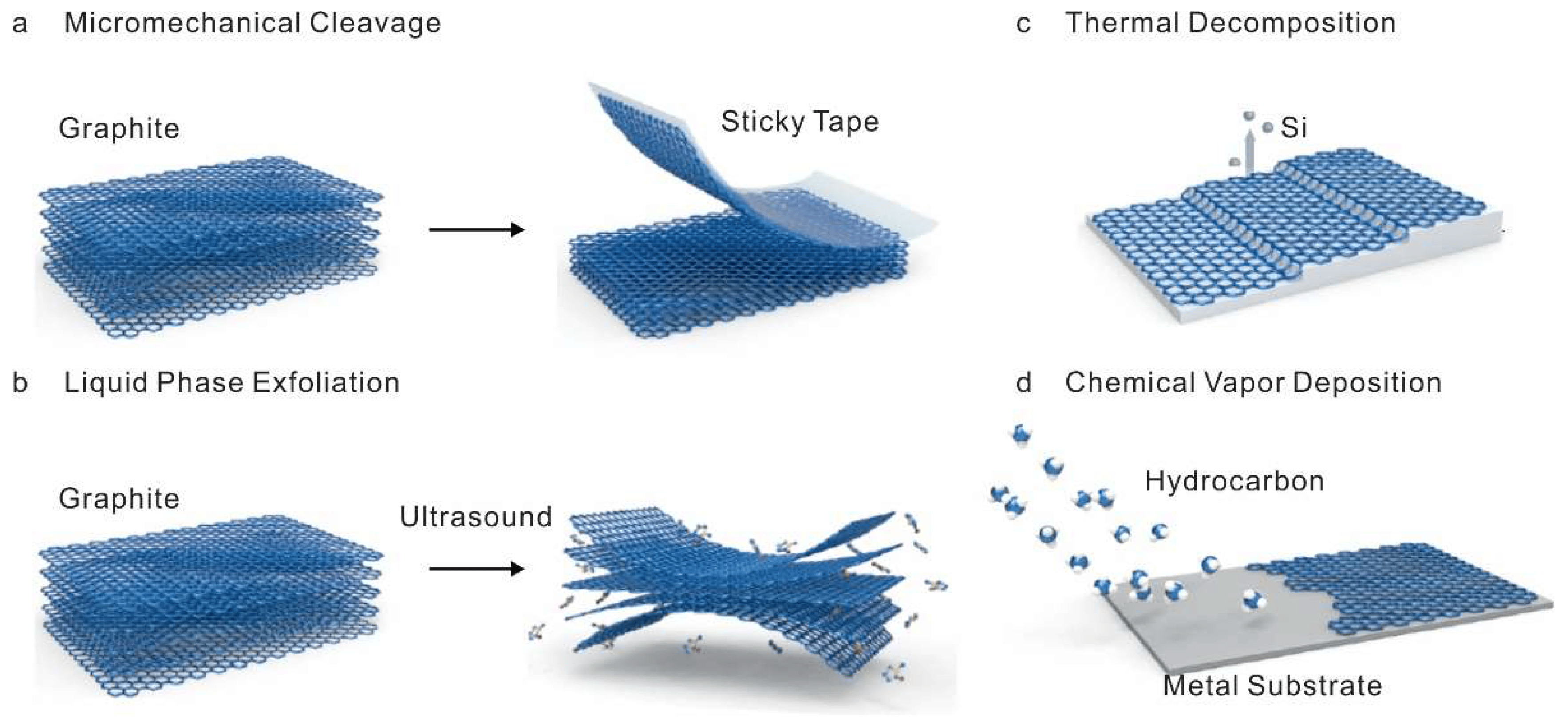
Figure 4. Schematic illustration of the graphene and its derivatives synthesis methods. (a) Mechanical exfoliation (b) liquid phase exfoliation, (c) thermal decomposition, and (d) chemical vapor deposition.
How to Make Graphene with a Blender?
The “recipe” of graphene in a blender emerged after the experiments of Jonathan Coleman, a professor at Trinity College in Dublin, in Ireland, and author of the study published in Nature Materials. Coleman, like many other scientists, was looking for cheap and simple ways to produce tons of clean and good quality graphene scales.
The team led by Coleman was funded by the British firm Thomas Swan. Basically, the scientists employed a kitchen mixer and added:
1. 10 to 25 ml of detergent
2. 500 ml of water
3. 20 to 50 grams of graphite powder, found on the tips of the pencils.
Coleman's "recipe" indicates that everything should be mixed for 10 to 30 minutes. Many flakes of graphene are obtained floating in the water. These scales are the size of microns, each one with the thickness of one nanometer (which corresponds to one billionth of a meter) and 100 nanometers long.
According to Coleman, the emulsion in the blender produces a balance between the surfactant and graphite. In the laboratory, it has been proven to separate graphene in centrifuges, spectrometers and electron microscopes, but the "recipe" in the blender was made at the end of the investigation, like a wink from the scientists. In fact, the central study was conducted in an industrial type, of great proportions.
What Type of Blender Does It Need?
For the experiment a 400-watt high power kitchen mixer was used, although for the main study, they used the industrial equipment, obtaining 5 liters of graphene scales floating in the water.
The idea of this work was to demonstrate how easy it can be to produce this great conductor in industrial quantities. Thomas Swan, who funded the research of Coleman and his team, soon patented the process and built a pilot factory to obtain graphene powder so that it could be mixed with other materials.
Currently, graphene flakes are produced industrially and are even sold in online stores. The problem is that the quality is very variable. Sometimes they are defective or mixed with chemicals that decrease their conductive capacity.
Note: The procedure is not recommended at home. This post is merely illustrative and informative, so the responsibility lies with you.
Graphene from Sugar
At Rice University, Texas, researchers produced graphene from sugar. A team of scientists from the University of Hong Kong is working to obtain graphene from organic waste and similar studies are underway in Europe. Using food waste to obtain useful materials would be a great advantage, also because food waste is the main component of urban waste, which becomes more abundant each year.
Currently, there are many methods, but none is "perfect" since, generally, those that provide high-quality sheets do not allow high production at a "reasonable" price. On the other hand, those that do allow a high production of monoamines, give rise to graphenes with more defects and therefore, with worse electrical properties. This is not necessarily negative since not all applications require the same degree of structural perfection.
The good news in this regard is that scientists are constantly working to make possible the large scale production of Graphene at an affordable rate.
Production Difficulties with Graphene
One of the most important challenges graphene faces, meanwhile, is large-scale production. In this race, there are already alternatives that will try to shade it, such as molybdenite. This competitor is being studied at the Swiss Federal Institute of Technology in Lausanne with satisfactory results to date.
Molybdenite allows to reproduce really small electronic components, solves problems such as the oxidation of the pieces, the loss of energy and the instability of performance in the devices, and also has a resistivity band that gives it the innate ability to conduct current sometimes.
Finally, not only is it possible to produce graphene in the laboratory and to see the individual carbon atoms, it is also possible to modify its structure to change its properties, to make it a "functional" material. Today carbon atoms are already being replaced with silicon atoms in order to create innovative electronic devices, but in the near future we can think of modifying the structure of graphene with molecules of biological interest for the development of new medical therapies.
But for graphene to be used on a large scale, it is necessary to find an economical way of producing it, and there is still work to be done on this. At the moment this material can be obtained by mechanically exfoliating a graphite or graphite oxide surface, but procedures are being studied to extract it from organic material.

Have you heard Nanografi's awarded graphene production method Greengraphene?
Part 5: Popular Graphene Products & Solutions
Graphene has a lot of products that have unique properties and have important applications in a variety of sectors. Let’s discuss a few of its products:
What is a Graphene Sheet?
The graphene sheet is a material with extraordinary properties and multiple applications. It is an ultra-thin sheet of carbon atoms, designed by two Russian researchers, Andre Geim and Kostya Novoselov. Thanks to this discovery, the researchers have received the Nobel Prize for Physics.
Andre Geim and Kostya Novoselov have risen to the headlines with the award of the Nobel Prize for Physics for the discovery of the Graphene sheet. The researchers used the peeling technique which consists of tearing off the layers of carbon with adhesive tape, until only one remain. In this way they succeeded in isolating the thinnest sheet in the world, no one else had previously managed to obtain sheets of the thickness of single atoms.
The single layer of Graphene is known as Graphene Sheet. From the electrical point of view, the Graphene sheet is an excellent conductor and can be "functionalized", to create semiconductors, which makes it suitable for use in microelectronics. Graphene sheet also has good thermal conductivity, which allows its use in cases where it is necessary to quickly extract heat from a source, as in microelectronics itself, since the circuits heat up. Graphene sheet has high elastic and mechanical properties (such as diamond) and for this reason, it can be used individually, or inside other materials to give them high mechanical and elastic properties.
Graphene Sheet Thickness
The thickness of the graphene sheet can be modified according to the requirements. The one that is usually used and offered by Nanografi is 35 micrometers. It is the finest material that can be found in the world. The size of the graphene sheet is 29 x 29 cm and the thermal conductivity is 580 W/mK. Moreover, the density of the graphene sheet is 1.82 g/cm 3. If you are looking for a graphene sheet of specific thickness and other characteristics, let us know and we will provide you exactly what you need. The graphene sheet has the same mechanical strength as Graphene.
How do you make graphene sheets?
The Graphene Sheet is made from graphite, the starting point of the process consists of the stacking of carbon sheets on top of one another and is the form we find in nature. What the two new Nobel Laureates did was to understand their peculiar characteristics in order to obtain them, precisely from graphite, making it available in ultra-thin layers, suitable for a variety of applications. But we understand better what graphene sheet is. It is a thin sheet of carbon atoms, organized in a " honeycomb " structure with very particular properties. So, to obtain the Graphene sheet, the mechanical exfoliation method which is also called the scotch tape method is usually employed. With the help of scotch tape, the thin sheet of graphene is produced at high mechanical strength. There are different types of Graphene sheets. It can be transparent and conductive. The graphene sheets are employed for a variety of purposes.
Graphene Nanotubes
Graphene nanotubes are small rolled sheets of graphite with nanometric diameters and lengths of microns. Graphene nanotubes have excellent electrical, mechanical, optical, chemical, and thermal properties for which they are preferred for increasing several products and also to generate new ones.
Graphene sheets can be rolled up to make Graphene nanotubes. The exceptional thermal, mechanical, electrical, chemical and optical properties of graphene nanotubes allow them to be used in a lot of applications. Such applications can obtain important benefits by incorporating graphene nanotubes. Flat screens used by nanotubes as field emitters, Composite materials reinforced with nanotubes, chemical and biological sensors to detect polluting elements. Generally, sectors such as electronics, materials, sensors, chemistry, biotechnology, mechanics, energy, Scientific and photonic instrumentation could be benefitted by the incorporation of graphene in many of the products.
Graphene Oxide
Study of materials has been fundamental throughout the history for the development of various technologies, for example; burning materials to produce fire, sharpening stones to produce spears or the tips of the arrows for hunting, or even the use of light materials that absorb high impacts to produce automobiles today. This has led the human being to carry out an in-depth study on the materials that surround him, and considering that carbon is one of the elements that can take various allotropic forms, the study of the same has caused a diverse range of materials, among which are graphene, graphene oxide and reduced graphene oxide.
Graphene is one of the most promising materials today since it has very useful properties; such as being a much harder material than a diamond, being an excellent conductor of electrical current and its malleability, the latter is very rare in this material since hard materials are usually very poorly malleable and very fragile. This provides a whole world of applications for this material as in the use of touch screens for cell phones.
On the other hand, reduced graphene oxide is an intermediate point between graphene oxide and graphene, since, with the reduction of graphene oxide, the model becomes much more similar to graphene, having similar properties, however, not being the same material, reduced graphene oxide is a worse electrical conductor than graphene and better than graphene oxide.
Let’s study the properties and some of the applications of graphene oxide and reduced graphene oxide.
Properties of Graphene Oxide
In the study of the materials it is important to know the model that governs the material, since, with this, we can obtain physical, chemical and mechanical properties of the material, giving the opportunity to possible applications for said materials. There are several reasons why this occurs, but the complexity of this material is paramount because it is amorphous, however, graphene oxide can generally be described as a two-dimensional sheet that contains honeycomb-shaped carbon atoms of bee with functional groups of hydroxide and oxygen.
Graphene oxide has some great features for example conductivity, which is dependent on its atomic and chemical structure. In general, graphene oxide films have resistance in a sheet with values of 10 12 Ω⁄sq or greater, this means that this material conducts very easily, which is a poor property for conductors, However, for dielectric materials, it is very useful.

Reduced Graphene Oxide
Graphene oxide (GO) is a two-dimensional material, considered as functionalized graphene with oxygenated groups. It is the main precursor for obtaining reduced graphene oxide, since it is susceptible to being reduced (removal of oxygenated functional groups through physicochemical processes) and/or functionalized to facilitate its interfacial interaction with other materials (polymers, inorganic nanoparticles, etc.) and form composite materials, or by self-assembling sheets to produce GO-based macroscopic materials. These hybrid materials have physicochemical properties superior to those of their individual components and are currently used for applications in water remediation, censorship, catalysis, photovoltaic cells, reinforcement material, biomedicine, etc.
How to produce Reduced Graphene Oxide?
The efficacy of chemical and thermal reduction to produce reduced graphene oxide (rGO) from GO was studied and a method was developed for the direct manufacture of graphene oxide microlistons by self-assembling GO sheets. The results on the chemical reduction of GO demonstrated the reducing and stabilizing nature of citric acid, for which a possible reduction mechanism was proposed.
The thermal reduction is carried out in an argon atmosphere, at temperatures between 200 and 1000 °C, supporting the GO in a copper foil (Cu). In a single step, a hybrid compound formed of CuO 2 or Cu particles covered by rGO supported on a matrix of the same material was obtained. It is important to note that it is possible to control the Cu phase as a function of temperature.
Regarding the self-assembly of the GO sheets, particles are added under acidic conditions to produce micropistons. A mechanism has been proposed to explain the GO self-assembly process in a solid-liquid interface.
Resistant, rigid, transparent, flexible, excellent conductor of electricity and heat. These, in short, are the main properties of Graphene, which has become an element of fundamental importance for research. The easy reproducibility at the industrial level is a further incentive towards experimentation and knowledge of what will probably be the main constituent of many applications of the future.
All these particular features make graphene potentially suitable for different types of applications. In the near future, possible uses could include the production of electrical components such as sensors, batteries, solar cells, touch-screens, integrated circuits, and even high-performance composite materials. Its potential would allow it to be used also in the water desalination process. Further research on graphene is important to know its physical, chemical and mechanical properties. With this information, we can see the possible applications that can be given to some specific material.
Graphene Nanoplatelets
Graphene Nanoplatelets are nanoparticles consisting of short stacks of platelet-shaped Graphene Sheets that are in a planar form. Graphene Nanoplatelets are excellent electrical and thermal conductors as a result of their pure graphitic. It can be used in sensors, supercapacitors, wearable electronics, EMI shielding and more.

CVD Graphene
Chemical Vapor Deposition (CVD) is a chemical process that is widely used in the manufacture of high-quality Graphene, CVD graphene films are highly transparent, cost-effective, conductive and highly scalable.
CVD graphene have wide range of applications. It can be used in catalyst, solar energy, graphene optoelectronics, plasmonic and nanophotonics, graphene semiconductor chips, conductive graphene film, biomaterials and bioelectronic applications.
Graphene Dispersion
Graphene Dispersion product comes with the process of dispersing or
suspending Graphene Sheets or flakes evenly in a solvent. Graphene is a highly
conductive material, and dispersion products can significantly enhance the
electrical and thermal conductivity of composites and coatings. Graphene
Dispersion products can increase the surface area of the material, providing
more opportunities for chemical interactions and making it suitable for
applications such as catalysis and sensing. It is suitable for coatings, energy storage, electronics, optoelectronics and biomedical applications.
Boron-doped Graphene
Boron-doped Graphene is a type of graphene that has been intentionally doped
with boron atoms to alter its electronic and chemical properties. Boron doping
in graphene can introduce p-type doping, which increases the concentration of
holes in the graphene structure and can lead to changes in its electronic
properties. This results in increased electrical conductivity, improved catalytic
activity, and other unique properties. Boron-doped graphene generally used in energy storage & batteries, sensors, fuel cells and photovoltaic applications.

Graphene Aerogel
Graphene Aerogels are materials that have elasticity and they can easily gain
their original form after some compression. In addition, the low density of
Graphene Aerogels enables them to be very absorbent. Graphene Aerogels can
absorb more than 850 times its own weight. This property means that it could
be useful for environmental clean-ups like oil spills. It is widespread for supercapacitors, li-ion batteries, environment purposes and solar cell applications.
Graphene Quantum Dots
Graphene Quantum Dots are nanoparticles with a size of less than 10 nm. They
have outstanding properties like exceptional biocompatibility, and electronic
and photoluminescence properties with a high surface-to-volume ratio. GQDs
can disperse in water very easily. GQDs energy band gaps can be adjusted by
varying their size. GQDs photoluminescence can be changed parallelly by
tuning the band gap. Graphene quantum dots are generally used in bioimaging, solar cells, LEDs, sensors, supercapacitors & micro-supercapacitors and drug delivery systems.
Holey Super Graphene
Holey Super Graphene known as graphene sheet contains a large number of
holes/pores. The locations of the holes are important. The distribution of the
holes must be uniform. Holey Super Graphene still holds the properties of graphene
but Holey Super Graphene has a higher surface area, ion diffusion capacity, chemical
reactivity, and fewer stacked nanosheets than graphene. Thanks to these
properties, holey graphene shows better electrochemical performance. It has variety of application areas.

Conclusion
In essence, while the wonder of graphene offers a glimpse into a revolutionary future, it is through the efforts of pioneering enterprises like Nanografi that this future will be realized. With continued investment, research, and collaboration across sectors, we can expect a world transformed by graphene's integration in the coming years.
To get to know us better and explore our products, visit our website.
References
Figure 1. Wikipedia, die freie Enzyklopädie. (2023). Graphen. In Wikipedia. https://de.wikipedia.org/wiki/Graphen
Figure 2. Nanografi Nano Technology (2023). https://nanografi.com
Figure 3. Graphene is the strongest material. Phys.org. https://phys.org/news/2008-07-graphene-strongest-...
Figure 4. Wang, X.-Y.; Narita, A.; Müllen, K. Precision synthesis versus bulk-scale fabrication of graphenes. Nat. Rev. Chem.2017, 2, 0100.
Recent Posts
-

Nanocomposites in Food Packaging
The utilization of nanocomposites in food packaging represents a significant advancement in the fiel …19th Apr 2024 -

What is the Difference Between 7075 and 6061 Aluminum Alloy?
When comparing 7075 aluminum alloy to 6061 aluminum alloy, it's essential to understand their disti …5th Apr 2024 -

Iron-Air Batteries: The Ultimate Guide
Iron-air batteries represent a significant breakthrough in energy storage technology, offering a sus …29th Mar 2024