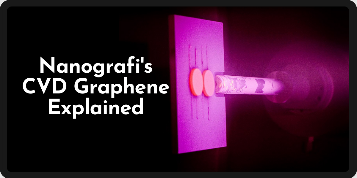
Nanografi's CVD Graphene Explained
Graphene has a structure of honeycomb and is a 2-d material. Its remarkable electrical, physical, and mechanical properties gained massive interest among different scientists. Graphene is also being used for organic photovoltaic cells (OPV) as flexible transparent due to high flexibility.
Since 2008-2009, Chemical vapor deposition (CVD) is the most important and valuable method for Graphene's preparation and production for a broad range of applications. Two steps help in the creation of CVD graphene, the formation of carbon by the precursor pyrolysis of material, and Graphene's carbon structure formation using the disassociated carbon atoms. CVD graphene films are highly transparent, cost-effective, conductive, and highly scalable. Overall, a great advantage is held by CVD graphene over ITO. In this article, two different kinds of investigations were viewed and done, the first one being the construction of thermos-electrochromic sensors and the second one being the synthesis and characterization of the CVD graphene. Two remarkable characteristics, the graphene layer's electrical properties, and thermochromic material's optical properties, when joined, can be implemented as an inner layer of ballistic covers or glass panes. All the applications are explained in detail here.
Introduction
Being an eye-catching material, Graphene has been tried in various optoelectronic devices to test, for instance, light-emitting diodes, solar cells, smart windows, supercapacitors, displays, sensors, or touch screens. Graphene has a structure of honeycomb and is a 2-d material. Its remarkable electrical, physical, and mechanical properties gained massive interest among different scientists. Also, Park and Ruoff have reviewed graphene production through methods of chemical exfoliation. Even though chemical and mechanical exfoliation, epitaxial growth on SiC can prepare Graphene, but the most important method for Graphene's production is the chemical vapor deposition (CVD) since being reported first in 2009 and 2008. Still, in reviews, graphene production through CVD hasn't been completely covered. Also, here we will review some of the representative and important CVD graphene applications, like Graphene being used for organic photovoltaic cells (OPV) as flexible transparent and Graphene being used for field-effect transistors (FETs).
Since 2008-2009, Chemical vapor deposition (CVD) is now the most important and valuable method for Graphene's preparation and production for a broad range of applications. For the monolayer graphene's growth with a high percentage of single layers, Cu has arisen as a good catalyst because of carbon's extremely low solubility in Cu. Different electrical properties are contained by CVD graphene that is very promising and valuable in a broad range of applications. For instance, on Ni, the growth of Graphene of few-layer can function for organic photovoltaic cells as flexible transparent conductive electrodes. Also, because on Cu foil, we can produce Graphene of large-grain, that has such electronic and mechanical properties that make them appropriate and applicable for being used in field-effect transistors
Production of CVD Graphene
There are two main methods of synthesizing Graphene: (1) the bottom-up method (epitaxial growth on different substrates, arc discharging methods, and chemical vapor deposition (CVD)) and (2) the top-down method (exfoliation, chemical oxidation, and mechanical exfoliation).
Two steps help in the creation of CVD graphene, the formation of carbon by the precursor pyrolysis of material, and Graphene's carbon structure formation using the disassociated carbon atoms.
1st stage is, the pyrolysis to disassociated atoms of carbon, should be carried out on the substrate's surface for preventing the carbon clusters (soot) precipitation during the gaseous phase. 2nd stage of producing the carbon structure out of the disassociated atoms of carbon, demands a massive heat level (without a catalyst over 2500 Celsius), therefore, in reducing the needed temperature to 1000 Celsius so that a reaction can occur, a catalyst is vital.
Properties of CVD Graphene
CVD graphene films are highly transparent, cost-effective, conductive, and highly scalable. Most importantly, their flexibility is very high, and therefore, they have promising applications in flexible OPV. Thus, a compromise of optical transparency and sheet resistance should be made so that OPV cell's best performance could be achieved. OPV cells using both ITO on PET, and Graphene on PET were side by side compared and fabricated.
Results revealed that the PET OPV cell/ CVD graphene displays an output power density that the ITO cells show of nearly 93%, also the CVD graphene film got a very high sheet resistance and very low optical transparency. As a control, the bending experiment was done with an ITO OPV cell to test the flexibility of graphene OPV cells. Due to ITO's brittle nature, the ITO device's illumination loss induced by bending is maybe related to micro-cracks.
Overall, a great advantage is held by CVD graphene over ITO because of the usage of transparent, conductive, and flexible electrodes in OPV cells.
Applications of CVD Graphene
It's because of its superior surface and electrical properties that, CVD method of preparing graphene film is way more promising and potentially suitable for the optoelectronic devices as compared to the method which includes reduced graphene oxide (rGO). To varied substrates, transferable of CVD graphene can happen, rendering this technique multipurpose for a broad range of applications.
One of its applications is in an inorganic (silicon) and organic solar cell as an electrode.
As electrons in the 2D lattice can only move in between carbon atoms, that makes CVD-graphene quasi-two-dimensional. For instance, one particular system of single mobile charge carrier is made as a result of the interaction of electrons with the atoms of carbon in the lattice. Carrier's ballistic moves over the surface of Graphene are known, thus allowing great conduction of electricity through graphene sheets.
In the article, two different kinds of investigations were viewed and done: (i) Construction of thermos-electrochromic sensors with CVD-graphene and their electrical characterization. (ii) Synthesis and characterization of the Graphene that's made through the method of CVD.
Preparation of Thermoelectrochromic Devices
In 1st attempt, from copper foil, Graphene was transferred by the method of high-speed electrochemical delamination onto a flexible substrate. Then the CVD-graphene substrate, which is flexible, was covered with different colors of four strips. As both the electrodes, thermally deposited gold (Au), was used in CVD-graphene's created devices.
To get more information about the applications of graphene,
you can read our blog post here.
Thermoelectrochromic Behavior of CVD-Graphene Device with Thermochromic Strips
Firstly, the possibility of thermochromic strips changing color because of the electro-modulation of Graphene's thermal properties was tested. Due to this, the investigation of the device happened, taking the voltage increase from 0 to 30 V into account. The multicolor layer changes its color with an increase in voltage and when the temperature is consequently applied. This assured that in sensors, CVD-graphene's thermal properties of electro-modulation could be used. As it is shown by the thermographic camera, due to an increase in the graphene layer's temperature, the selected strips change their color along with the increase in voltage. Reversible effects were displayed by our CVD-graphene device, and it's proved to be stable in the air atmosphere. Here, used strips are time- and air-stable and reversible change in color is shown by them along with the change in temperature. For explaining this effect, a commercially available Peltier device was used to change the strip's temperature. The advantage lies in Graphene's electric properties, which, specifically here, are very beneficial: implementing voltage to the layer of Graphene through electrodes leads to an increase in the temperature of the layer. Previously having a color and implementing as a cover for the structure of Graphene, the electrochromic layer is now colorless (transparent). A PET made flexible substrate (base layer) having these layers layered on them, for instance, permits the sensor to adapt to the object's surface that is to be monitored. By using either a current/voltage meter for voltage/current characteristics, an unaided eye and thermal imaging camera, we can observe the resultant changes (damage), because the thermochromic material's color change is visible.
In short, the invention can be used as a sensor that assures the location and the presence of damage to, for instance, automotive glazing, shop window panes, helicopters' ballistic covers, flak jackets, or bulletproof vests. Through this sensor, the safety level can be checked, and the user's safety, for example, of police officers, ordinary citizens, and soldiers, can be improved remarkably. This shape and structure can be provided as an example of joining two remarkable characteristics, the graphene layer's electrical properties and thermochromic material's optical properties, which can be implemented as an inner layer of ballistic covers or glass panes.
Transfer of Graphene Films
To facilitate Graphene for applications of photovoltaic or nanoelectronic, remove substrates of catalytic metal from Graphene and then transfer Graphene onto the arbitrary substrates. Firstly, a thin layer of polymethyl methacrylate (PMMA) coats Graphene, and then at 102 C, it's baked for solvent evaporation. Cu or Ni etchant removes the layer of metal, leaving behind only the graphene/PMMA film. Deionized (DI) water cleans the film and then transfers it onto a targeting substrate. Acetone removes PMMA after water vapor evaporates, leaving a film of Graphene on targeting the substrate's top. Both full wafer graphene was able to transfer from Cu foil and Ni film onto glass using the above-mentioned method, Si/SiO2 substrates, and polyethylene terephthalate (PET) films.
Graphene Photovoltaic Cells
Films of Graphene are highly flexible, conductive, and transparent, which are measured to be possible and promising candidates in photovoltaic cells for transparent conductive electrodes. Indium tin oxide (ITO) as anode material is used typically by the conventional OPV cells because of its high transparency and very low sheet resistance (∼25 Ω/sq). Still, indium's scarcity reserves and metal oxides' highly brittle nature enforce serious limits on the ITO's use for such applications where mechanical flexibility, physical conformation, and cost has great importance.
Large-Grain Graphene and Graphene Transistors
Cu foils and Ni films have films of continuous CVD graphene synthesized on them, and they are generally polycrystalline, and their grain size is small (some micrometers). As the boundaries of grain between each Graphene's grain impact both mechanical and transport properties negatively, thus it is very important to synthesize single-crystalline, large-grain Graphene for facilitating Graphene's applications.
For synthesizing single-crystalline, large-grain Graphene, the method of vapor-trapping is developed. For growth, CH4/H2 was flown into a tube of large quartz (2 in.), and Cu foil was loaded into a tube of small half-inch quartz.
Relatively, Cu foil that's located outside the tube that wraps vapors and continuous graphene film can be shown by Graphene grown on the foil of Cu with a little etching. In between the two results of growth, there is a great difference indicating that in changing the tube's local environment, a significant role is played by the vapor trapping tube. Quasistatic reactant gas distribution' creation and carbon supply reduction leads to graphene grains of the shape of a large flower. Graphene flowers of large-grain were transferred onto the substrate of Si/SiO2, and micro-Raman microscopy characterizes them.
Conclusion
Here, the graphene film's chemical vapor deposition on Cu and Ni is reviewed, and the difference between the mechanisms of graphene growth on Cu and Ni is also debated. Here, two important and interesting applications are achieved, one is multilayer graphene films as transparent, flexible. The second is for OPV cells as conductive anode material and synthesis of Graphene of large-grain and its application for field-effect transistors on substrates of both h-BN and Si/SiO2. Also, the growth of Graphene at low temperature will be attractive for cost reduction. A deeper knowledge of the chemistry of graphene growth is required.
To get more information, you can visit Blografi.
References
https://www.graphenea.com/pages/cvd-graphene
https://www.intechopen.com/books/graphene-materials-advanced-applications/fundamentals-of-chemical-vapor-deposited-graphene-and-emerging-applications
https://www.hindawi.com/journals/jnm/2017/2757590/
Recent Posts
-
What is the Difference Between 7075 and 6061 Aluminum Alloy?
When comparing 7075 aluminum alloy to 6061 aluminum alloy, it's essential to understand their disti …5th Apr 2024 -
Iron-Air Batteries: The Ultimate Guide
Iron-air batteries represent a significant breakthrough in energy storage technology, offering a sus …29th Mar 2024 -
Discovering the Power of 2D Materials
In material science, the discovery of two-dimensional (2D) materials represents a transformative de …22nd Mar 2024


