 for a Better Future")
Nanoelectromechanical Systems (NEMS) for a Better Future
The nanoelectromechanical systems precisely known as NEMS are a group of certain devices that possess both the traits of electric and mechanical functioning at rather a minor scale.
They possess nanoparticles that are so small that they cannot be seen with an ordinary microscope and instead an electron microscope is used to view these materials. It is because of the size that they hold which is equal to the size of a grain and has a very high fraction as well. The natural production of nanoparticles is done by many geological, cosmological, meteorological, and biological processes. NEMS has some remarkable properties, a large quantum mechanical effect being the most prominent, efficient, and highlighted one. Likewise, their applications too, are remarkable and NEMS is being applied in various fields. Moreover, the exceptional properties of NEMS lead to significant advances in various fields, leading us to innovative applications in Nanografi's advanced materials.
Introduction
A class of devices known as Nanoelectromechanical systems (NEMS), integrates functionality both mechanically and electrically, on the nanoscale. The next step of logical miniaturization is formed by NEMS via MEMS devices or commonly known microelectromechanical systems. Nano-electronics that are like transistors are integrated typically by NEMS with motors, pumps, and mechanical actuators and therefore, chemical, physical, and biological sensors are formed.

An Overview of Nanoelectromechanical Systems (NEMS)
The name is derived from the dimensions of the device, typically in the range of nanometers, resulting in potentially large quantum mechanical effects, high mechanical resonance frequencies, and low mass, for instance, a high ratio of surface-to-volume, zero-point motion, both beneficial for the sensing mechanisms that are based on surface. It has many applications, some being as accelerometers and detecting the chemical substance in air, sensors. NEMS technology uses many common materials, most of which are based on carbon, especially graphene, carbon nanotubes, and diamond. NEMS needs are directly met by carbon-based materials as their characteristics are very useful. Carbon’s mechanical characteristics (for instance, large Young's modulus) are very important for NEMS stability meanwhile the carbon-based material's semiconductor and metallic conductivities enable them to act as transistors.
Large surface area, high young’s modulus, low friction, low density, and very low mechanical dissipation are displayed by both diamond and graphene. CNT's low friction enables practically frictionless bearings, and in CNT's practical applications, it is a big enough motivation, for instance, in NEMS as constitutive elements, like high-frequency oscillators, switches, and nanomotors. The physical strength of graphene and carbon nanotubes permits the materials that are carbon-based to meet huge demands of stress, on which any typical material would fail and therefore, as significant materials, supports their usage in the technological development of NEMS.
Along with carbon-based materials' mechanical advantages, in many NEMS’ electrical components, graphene and carbon nanotube’s electrical characteristics permit its usage. For both graphene and carbon nanotubes, the development of nano transistors has been done.
Background
In 1959, Richard Feynman said that at the bottom, the room is plenty. At smaller sizes, the potential applications are many, and if devices are produced and controlled at smaller scales, all technology benefits. The advantages that we are counting on are reduced size, greater efficiencies, reduced power consumption, and lower production costs in electromechanical systems.
In 1960, MOSFET was fabricated for the first time with 100 nm gate oxide thickness. In 1962, a nanolayer-base metal-semiconductor junction (M–S junction) transistor using gold (Au) thin films with 10 nm thickness was fabricated. Starting with the FinFET, scaling was enabled by the multi-gate MOSFETs below a channel length of 20 nm. In 1998, at UC Berkeley, FinFET devices were fabricated down to a channel length of 17 nm.
At IBM, in 2000, the researchers for the first time demonstrated the very-large-scale integration (VLSI) device of NEMS. Its premise was an AFM tip’s array that can sense/heat a deformable substrate for functioning as a memory device.
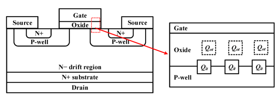
Figure 1. Structure of the MOSFET and the gate oxide layer.
Properties of Nanoelectromechanical Systems (NEMS)
Devices that are based on NEMS display different characteristics and features heralding a new era in the sophistication of technological applications.
High Mechanical Resonance Frequencies: NEMS devices can achieve remarkably high mechanical resonance frequencies. This is due to their small size, which allows for rapid oscillations. High resonance frequencies make NEMS ideal for a wide range of applications, including highly sensitive sensors, filters, and resonators.
High Electrical Strength: These devices exhibit high electrical strength, allowing them to withstand significant voltages without breaking down. This property is crucial for their reliability and efficiency in electrical applications, including actuators and transducers.
Low Mass: The tiny scale of NEMS devices results in extremely low mass. This low mass contributes to their high resonance frequencies and also means that they require very little energy to operate. This makes NEMS devices particularly suitable for applications where power consumption is a critical factor.
Large Quantum Mechanical Effects: NEMS operate on a scale where quantum mechanical effects become significant. For example, zero-point motion — the lowest possible energy state of a quantum mechanical physical system, distinct from the classical minimum energy state — can be observed in NEMS. This quantum characteristic opens up possibilities for new technologies and applications, such as quantum computing and quantum sensing.
High Surface-to-Volume Ratio: NEMS devices have a high surface-to-volume ratio, which is advantageous for surface-based sensing applications. This feature allows for greater interaction with the environment, making NEMS excellent candidates for sensitive chemical, biological, and environmental sensors. The large surface area relative to volume enhances the device's responsiveness to surface-bound events, improving sensitivity and selectivity.
Applications of Nanoelectromechanical Systems (NEMS)
Nanoelectromechanical Relay
Through the usage of methods for semiconductor fabrication, a nanoelectromechanical (NEM) relay is built on the nanoscale. NEM relay is a switch that is electrically actuated. When in conjunction, or in replacement with traditional semiconductor logic, they operate because they are designed to do so. Despite, NEMs' mechanical nature to switch slowly as compared to solid-state relays, NEMs have many benefits, for instance, consumption of less power and leakage of no current, all these benefits make NEMs beneficial and potentially important in computing of the next generation.
10 or more volts are required by a typical NEM Relay for pulling in, and on gigaohms, have contact resistances. Platinum-coated contact surfaces have achievable contact resistance lessened to at least 3 kΩ. In comparison with transistors, NEM relays switch gradually and slowly in nanoseconds order.
Nanoelectromechanical Systems (NEMS) Mass Spectrometer
To measure the analyte particle's mass, an instrument like a nanoelectromechanical systems mass spectrometer (NEMS-MS) is used. NEMS-MS measures by observing on NEMS resonator, frequency shift which is the result of the particle adsorption. In 1999, at the California Institute of Technology, NEMS-MS was invented.
Nanoelectromechanical-based Cantilevers
With very high frequencies (VHF) of mechanical resonance, a cantilever based on NEM was developed by researchers from the California Institute of Technology. Efficient and unambiguous nanodevice readout is facilitated by the incorporation of electronic displacement transducers which are piezoresistive thin metal films-based. The surface of the device is made functional through the usage of a thin polymer coating with a high partition coefficient for the targeted species, it enables the cantilevers that are based on NEMS for providing measurements of chemisorption at room temperature with the mass resolution at less than one attogram. Cantilevers that are based on NEMS have some more capabilities which are used for the applications of scanning probes, sensors, and very high-frequency operating devices (100 MHz).
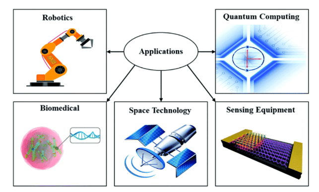
Figure 2. Future applications of 2Dm NEMS resonators.
A Better Future with Nanoelectromechanical Systems (NEMS) Applications
Nanoelectromechanical Systems (NEMS) Based Applications
Widely, Nanoelectromechanical Systems NEMS market's application segmentation is categorized into 3 groups; solid-state electronics, sensing and control, and tools & equipment. Further, each of these applications is separated into level two applications, for instance, memories, automotive, sensors, microscopy, and medical. All application analysis includes value/volume data, the penetration rate in the existing market, and an estimation of the commercialization year. Qualitative data only is included by the segmentation that is based on technology. As the NEMS technology is improving and changing, the quantitative part is being avoided, thus errors will be induced by forecasting for the evolving technology.
Nanoelectromechanical Systems (NEMS) Based on Products
According to many product types, the market is segmented, for instance, nano-fluidic, nano-cantilevers, nano-tweezers, and nano-accelerometer modules. Many different components manufacture these products. Based on the applications in which the products are used, the products are categorized.
NEMS Based on Components
The segmentation of the market on numerous nano components basis has also been showed. To synthesize various nanoproducts, numerous nano-components are used. In the report, nano-components are covered, for instance, nanobelts, nanowires, nanotubes, and nanofilms.
NEMS Based on Materials
In the materials chapter, the 17 raw materials which are highly used for the production of NEMS are covered. All of them are categorized into 3 categories; insulators, semiconductors, and metals. Therefore, it is said that for the report, the entire market breakdown of the NEMS market’s supply side is done.
NEMS Based on Geography
Even against geography, the market of NEMS is mapped. From a geographical point of view, further, the market is segmented into ROW, Europe, North America, and APAC, giving us a brief overview of the potential regions for markets NEMS. Also, concentrated regional pockets are explained in the report as they are very important when it comes to the generation of revenue.
The nanoelectromechanical system is the full form of NEMS. Further, the feature of miniaturization is extended by NEMS towards the individual molecules and atoms' limits. At the level of a nanometer, the devices that are based on NEMS stand on the movement. Below or at 100nm, in comparison with the microelectrochemical systems, NEMS is considered to be the elements of structure, meanwhile MEC systems are at a scale of micrometer length. Due to NEMS's most remarkable properties, for instance, the higher ratio of surface area to volume, higher electrical efficiency, and smaller mass, it is good for applications that are highly efficient like ultrasensitive sensors and high-frequency resonators.

The use of graphene is especially common in NEMS technologies. Learn now.
What is the Future of Nanoelectromechanical Systems (NEMS)?
There are some main problems right now in the application of NEMS devices commercially, for instance, reasonable low integrations of products that are carbon-based should be made. Recently, for the diamond, a step is made in that direction to attain a level of processing like that of silicon. Now, from the experimental work, attention is shifting toward the structure of the device and practical applications. From these novel devices, device structure will implement and profit. Overcoming the next hurdle involves understanding these carbon-based tools' properties, and then using them for making durable and efficient NEMS with less rate of failure.
For the usage of NEMS, carbon-based materials have played a role due to their remarkable electrical and mechanical characteristics. By 2022, $108.88 million is supposed to be reached by NEMS global market. Hopefully, it is predicted that in applications of high frequency, NEMS will be above MEMS in the coming 10 years because of the NEMS having a high resonating frequency in the GHz range. The other good reason for NEMS to be more successful is low power consumption. A significant breakthrough is brought about by devices of NEMS in the way of manufacturing and designing systems, devices, and materials. The miniature device can be controlled by electronic circuitry combined with mechanical elements, for instance, cantilevers, actuators, and sensors with the aid of numerous methods of nanofabrication. In the NEMS, the electrical characteristics are combined at the nanoscale with the mechanical components for developing devices that can perform tasks, which is not possible through the usage of conventional technologies.

Conclusion
Though the devices having NEMS have fairly a lot of advantages and applications but the holdback that NEMS will face in the future is that they have fairly fewer carbon-based products. So, to have a better future with the NEMS devices research and ongoing works are being carried out to eradicate all the hurdles that might suppress their production and usage.
To discover the latest articles in environmental applications of nanotechnology, you can visit Blografi.
References
Commercial Value and Benefits of Carbon Nanotubes Transistors - Nanografi Nano Technology. (n.d.). Retrieved March 12, 2024, from https://nanografi.com/blog/commercial-value-and-benefits-of-carbon-nanotubes-transistors/
New Market Reports. (n.d.). Retrieved March 12, 2024, from https://www.marketsandmarkets.com/new-reports.asp
Solid-state Silicon batteries Properties and Applications. - Nanografi Nano Technology. (n.d.). Retrieved March 12, 2024, from https://nanografi.com/blog/solidstate-silicon-batteries-properties-and-applications/
Structure of the MOSFET and the gate oxide layer. | Download Scientific Diagram. (n.d.). Retrieved March 12, 2024, from https://www.researchgate.net/figure/Structure-of-the-MOSFET-and-the-gate-oxide-layer_fig1_366196619
The Best Way to Utilize Carbon Nanotubes in Industry with Potential Applications - Nanografi Nano Technology. (n.d.). Retrieved March 12, 2024, from https://nanografi.com/blog/the-best-way-to-utilize-carbon-nanotubes-in-industry-with-potential-applications/
Young’s modulus - Wikipedia. (n.d.). Retrieved March 12, 2024, from https://en.wikipedia.org/wiki/Young%27s_modulus
Recent Posts
-

Nanocomposites in Food Packaging
The utilization of nanocomposites in food packaging represents a significant advancement in the fiel …19th Apr 2024 -

What is the Difference Between 7075 and 6061 Aluminum Alloy?
When comparing 7075 aluminum alloy to 6061 aluminum alloy, it's essential to understand their disti …5th Apr 2024 -

Iron-Air Batteries: The Ultimate Guide
Iron-air batteries represent a significant breakthrough in energy storage technology, offering a sus …29th Mar 2024