 Wafer: Structure, Properties, Uses")
Gallium Arsenide (GaAs) Wafer: Structure, Properties, Uses
Gallium Arsenide (GaAs) Wafer is a significant type III-V direct bandgap semiconductor used in various devices such as infrared emitting diodes, laser diodes, and microwave frequency integrated circuits. It is also utilized in the production of photovoltaic cells.
On the other hand, Gallium Arsenide Wafers, the commercially available form of GaAs, hold an integral role in the semiconductor industry. They primarily serve as platforms or substrates in an epitaxial pattern for the growth of additional semiconductor materials. Their technical uses include the integration of type III-V semiconductors and high-performance optoelectronic devices like high-density p-i-n detectors and laser diodes with robust silicon electronic integrated circuits. This integration is done monolithically to create durable circuits with a range of applications. Nanografi's Gallium Arsenide (GaAs) wafer products provide excellent signal transmission in high-frequency applications, thanks to their high performance and wide bandwidth.
Introduction
Gallium arsenide (GaAs) is a compound of gallium and arsenic. It is a vital semiconductor and is commonly used to manufacture devices such as infrared emitting diodes, laser diodes, integrated circuits at microwave frequencies, and photovoltaic cells.
Gallium arsenide (GaAs) wafers are crucial components in the manufacturing of various electronic devices. These wafers consist of single crystals of gallium arsenide, possessing unique electrical and optical properties. GaAs wafers are typically grown using techniques like molecular beam epitaxy (MBE) or metalorganic vapor phase epitaxy (MOVPE). GaAs is a III-V compound semiconductor with a direct bandgap, allowing for efficient emission and absorption of light in the infrared and visible light spectrum. GaAs wafers have high electron mobility, surpassing that of silicon, making them suitable for high-speed applications such as microwave devices, high-speed transistors, and integrated circuits (ICs).

Structure of Gallium Arsenide (GaAs) Wafer
In the Gallium arsenide (GaAs) wafer, each gallium atom is bordered by arsenic atoms. 5 valence electrons of arsenic atoms and 3 valence electrons of gallium atoms share each other. So, each of the gallium and arsenic atom gets 8 valence electrons in the outer shell. It is also to be noted that a covalent bond exists between gallium and arsenic atom in the GaAs Wafer. The covalent bonds despite being strong can be broken with an enough amount of external energy.
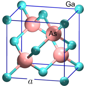
Figure 1. The structure of Gallium arsenide wafer. The As and Ga atoms are represented by large pink and small green spheres, respectively.
Preparation Methods of Gallium Arsenide Wafers
Vapor-phase Epitaxial (VPE) growth method: VPE is a method to deposit several layers of material onto a substrate. In this method, a volatile precursor undergoes a chemical change at a surface, resulting in a solid deposit. The reaction can be enhanced by the addition of gases such as hydrogen or argon. This technique can produce highly uniform films with good material properties.
Gradient Freeze (GF) method: This method is often used for creating single-crystal materials. As you described, the process involves carefully controlling the temperature in the furnace to gradually solidify a melt, which allows for the formation of a single crystal. The benefit of this method is that the crystal that's produced is typically high-quality and has a low defect density.
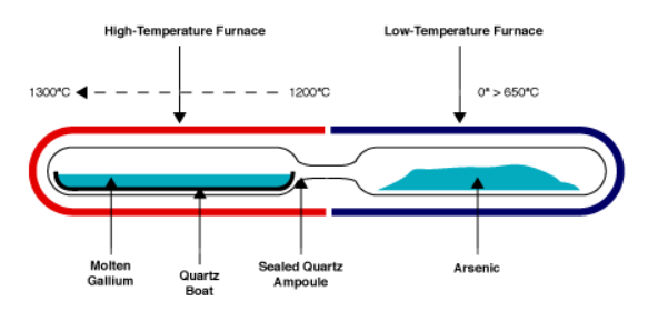
Figure 2. Gallium arsenide synthesis by horizantal gradient freeze.
Liquid-phase Epitaxial (LPE) growth method: LPE is a method used to grow single-crystal semiconductor layers from a melt on a substrate. It's often used for manufacturing components of electronic and optoelectronic devices, such as LEDs.
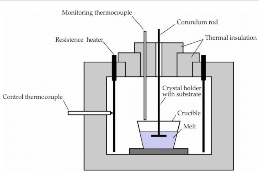
Figure 3. Experimental set-up for liquid-phase epitaxy (LPE).
Liquid-encapsulated Czochralski (LEC) method: This technique is used to grow single crystals of materials, particularly semiconductors such as gallium arsenide. The crystal is drawn from a melt which is contained within a suitable crucible and is protected from contamination by being encapsulated by a liquid, hence the name.
Molecular Beam Epitaxy (MBE) and Metal-Organic Chemical Vapor Deposition (MO-CVD): These are newer methods of creating gallium arsenide wafers. MBE involves the interaction of a beam of one or more thermalized elemental or compound sources with a heated surface. Metal-organic chemical vapor deposition is a versatile technique for growing thin films of a variety of materials. Both of these techniques allow for the growth of highly controlled, high-quality layers of material.
Bridgman-Stockbarger technique: This is another method for growing single-crystal materials. The basic premise involves moving the material to be solidified slowly through a temperature gradient. At the hot end, the material is molten, and at the cold end, it's solid.
Properties of Gallium Arsenide (GaAs) Wafer
The main properties of gallium arsenide (GaAs) are given below:
- The Molar mass of Gallium arsenide (GaAs) is 144.64 g/mol.
- Gallium arsenide (GaAs) has the Melting point of 1238 °C.
- The density of Gallium arsenide (GaAs) is 5.32 g/cm3.
Use of Gallium Arsenide (GaAs) Wafer
The main use of gallium arsenide (GaAs) is found in:
- Computers
- Photovoltaic cells
- Optoelectronic communications
- Laser diodes and infrared emission
GaAs Wafers' Use in Transistors & Computers
Gallium arsenide wafer, a binary compound formed from the element gallium and arsenic, presents manufacturing challenges in the production of transistors due to its lower thermal conductivity and higher coefficient of thermal expansion (CTE) compared to elementary semiconductors like silicon and germanium. Additionally, understanding device failures based on GaAs can be more complex and costly than those based on silicon due to its relatively recent adoption. However, when considering the balance of quality, price, and the added value of GaAs, these complications are outweighed. The growing markets, demanding technology that enables higher frequencies, contribute to the offset of these costs.

GaAs Wafers' Use in Defense & Aerospace
Gallium arsenide has been incorporated into commercial marketssince its use began for the military and aerospace field. It belongs to the semiconductor materials group in the periodic table. The width of the band gap is greater than in silicon or germanium. The mobility of the electrons is also greater than in silicon or germanium, and that of the holes similar to those of silicon.
To impurify the type p, materials such as zinc, cadmium or copper are used since they introduce permitted levels in the range of 0.08 to 0.37 eV above the valence band of GaAs. The donor materials are sulfur, selenium and the elements of group IV of the periodic table, in small concentration, if they replace gallium atoms.
The GaAs is used for photoelectric cells, tunneling diodes, lasers, semiconductors and MESFET transistors.
The GaAs has several circuit topologies and device types. The most dominant and commercially available is the FET logic directly coupled with DCFL (Direct Coupled FET Logic), although BFL logic (Buffered FET Logic) and SDFL logic (Schottky Diode FET Logic) are also available
GaAs Wafers Use in High frequency Technologies
The effective mass of the electric charge of the doped N-type GaAs is lower than in the silicon of the same type, so the electrons in GaAs Wafers are accelerated at higher speeds, taking less time to cross the transistor channel. This is very useful at high frequencies, since a higher maximum operating frequency will be reached.
This possibility and need to work with circuits that allow to act at higher frequencies has its origin in the defense and space industries, in the use of radars, secure communications and sensors. After development by federal programs, GaAs soon expanded to new commercial markets, such as wireless local area networks (WLAN), personal communication systems (PCS), live satellite transmission (DBS), transmission and reception by the consumer, global positioning systems (GPS) and mobile communications. All these markets required working at high and low frequencies that could not be achieved with silicon or germanium.
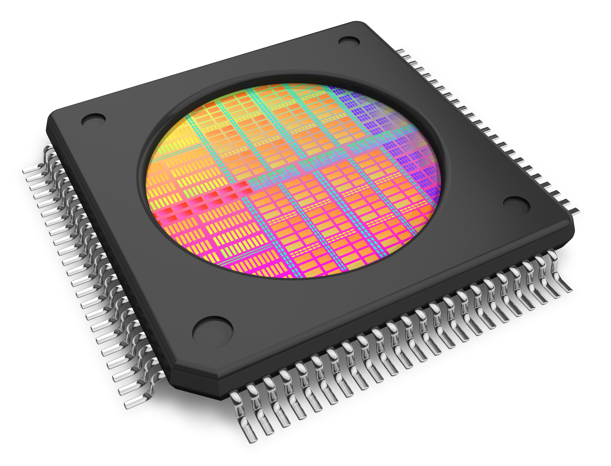
Figure 4. GaAs in high-frequency technology applications.
Advantages of Gallium Arsenide (GaAs) Wafers
The advantage of gallium arsenide wafers over solar-grade silicon wafers is that it offers almost twice the efficiency. Another advantage of GaAs wafer refers to the increase in efficiency. Usually the gallium arsenide is deposited in a single thin layer on a small sheet, but at the University of Illinois, multiple layers of material have been deposited on the wafers, obtaining a higher yield. Multiple layers eliminate the limitations in the area of work, something very important in the case of solar cells, which require a wide coverage area to capture as much light as possible. Thus, a greater area of coverage is achieved, generating more energy and lower cost. The use of arsenide in solar cells is not new. It has been used for many years in the multi-junction cells.
Disadvantages of Gallium Arsenide (GaAs) Wafers
The devices manufactured with GaAs wafers can work at temperatures of up to 450 °C. But despite this advantages, its use poses some difficulties, compared with that of silicon. For example, unlike silicon, there is no natural oxide that acts as a mask to produce simple elements of the CMOS logic style.
The big disadvantage, which explains its low utilization, is the price. To solve this dilemma, engineers and researchers say they have achieved new methods of manufacturing thin films of low cost gallium arsenide, which would create devices that would replace silicon, hence in
creasing the efficiency of photovoltaic cells.
Conclusion
Gallium arsenide (GaAs) contains an atom of Gallium and another atom of Arsenide. Its use is commonly found in electronics, such as in the manufacturing of semiconductors. The compound has some advantages and disadvantages, as described above. The work is underway to regulate the price of this compound and there is much more that Gallium arsenide (GaAs) Wafers can offer in other sectors also. Therefore, the research must be continued to discover its exceptional uses. Visit Nanografi to enhance your projects and research and discover our cutting-edge products.
References
https://nanografi.com/blog/gallium-specifications-...
https://nanografi.com/blog/properties-and-applicat...
https://www.researchgate.net/figure/Color-online-T...
https://en.wikipedia.org/wiki/Monolithic_microwave...
https://www.waferworld.com/post/gaas-wafer-major-u...
http://ece-research.unm.edu/jimp/vlsi/slides/chap5...
https://www.researchgate.net/figure/Scheme-of-the-...
https://www.sciencedirect.com/topics/chemistry/vap...
Recent Posts
-

What is the Difference Between 7075 and 6061 Aluminum Alloy?
When comparing 7075 aluminum alloy to 6061 aluminum alloy, it's essential to understand their disti …5th Apr 2024 -

Iron-Air Batteries: The Ultimate Guide
Iron-air batteries represent a significant breakthrough in energy storage technology, offering a sus …29th Mar 2024 -

Discovering the Power of 2D Materials
In material science, the discovery of two-dimensional (2D) materials represents a transformative de …22nd Mar 2024