
Cz-Si Wafers: History, Properties, Applications
Czochralski Silicon (CzSi) wafer is an important wafer of Silicon. Silicon (Si) is a chemical element which comprises about 30 percent of the earth’s crust. Right after oxygen, it is the commonest natural element in the world and often used in building microchips and semiconductors. Unlike other elements like hydrogen, silicon is not a very good conductor of electricity as a whole. Although, a semiconductor can be built only when silicon has been transformed into liquid or water.
Silicon wafers are commonly used in the formation of a large number of semiconductor devices. For several decades, Si has had a guiding influence over the electronics and semiconductors industries. Most of them are used for commercial purposes as a whole with little or no processing. Examples of such usage are industrial construction with stone, silica, and clay. Czochralski Silicon (CzSi) wafer are also used in the production of mortar, stucco concrete (mixed with the silica sand). They are used in the creation of ceramics, especially glasses. Some of its compounds are used as abrasives.

Properties and characteristics of Cz-Si Wafers
The properties and characteristics of a Czochralski Silicon (CzSi) wafer basically cover those criteria or requirements that a silicon wafer must satisfy to be termed as such. These properties include electrical, mechanical, chemical and surface features.
1. Flatness of Cz-Si Wafers: depending on its application, these wafers are usually flat. A flatness of 1-3 microns is acceptable.
2. Size of Cz-Si Wafers: the size of a Czochralski Silicon (CzSi) wafer has continued to increase, having a diameter of 300mm max.
3. Thickness of Cz-Si Wafers: A wafer with a larger size must be thicker. However, if there must be an increase in its thickness, such an increase must be less than the increase in diameter.
4. Shape of Cz-Si Wafers: Czochralski Silicon (CzSi) wafers are usually circular in shape, while its dies are rectangular or square-shaped.
5. Orientation Notches: Usually, a wafer may contain one or more notches which provide more information about the wafer. Those that are lower than four inches utilize two notches at different points, revealing the orientation of their crystallographic surface and their type of semiconductor. However, wafers with a diameter of four inches, have just one notch which reveals their orientation.
6. Impurity doping: Czochralski Silicon wafers are not totally pure silicon, rather, they are formed with an impurity doping mixture of atoms (boron, arsenic, antimony or phosphorus) which are added to the concentration while categorizing the wafer as either p=type or n=type
7. Cracks: A Czochralski Silicon (CzSi) wafer should be free from damage and all kinds of roughness to become qualified for high performance. Therefore, damaged parts have to be removed notwithstanding a rough top layer.
History and Origin of Cz-Si wafers
The history of Czochralski Silicon (CzSi) wafer cannot be discussed without first of all tracing the history of silicon itself. The history of silicon can be traced to the discovery made by Jons Jacob Berzelium, a chemist from Sweden, as far back as 1824. However, it had no substantial use by major industries until the late 1940s when companies began creating transistors using a similar material, Germanium (Ge). However, in the early 1950s, silicon was found to be a better semi-conducting material than the initial germanium.
By its very nature, silicon reduces operating temperatures while increasing power output. In 1954, silicon became the sole agent responsible for enabling the small version of electronics. At present, most memory chips, solar cells, and transistors are produced using silicon, which takes the form of wafer slices obtained from a silicon ingot. The growth of a silicon ingot takes about a week to one month, depending on a number of factors. Majority of silicon wafers are developed through the Czochralski (Cz) process. These ingots demand a large amount of pure polycrystalline silicon, which is put in a crystalline crucible together with some quantities of elements called dopants (the commonest dopants are antimony, arsenic, and phosphorus). Once the ingot becomes fully developed, it is ground to an amorphous size which is a bit larger than the target size or diameter of the last silicon wafer. As soon as the wafers have been completely sliced, the process of lapping begins to get rid of marks and defects obtained during the slicing process.
Applications of Cz-Si Wafers
Czochralski Silicon (CzSi) wafer have a lot of uses. Some of its applications include manufacturing or production of semiconductors; manufacturing of smartphones and other computers; creation of home appliances; manufacturing of solar cell; drone technology and aerospace; microchips; transistors, calibrating instruments; integrated circuits; electronic components; sensor devices and so on. Some of these are discussed below:
CzSi wafers as a semiconductor
Silicon is the commonest semiconductor due to its high mobility in high and low temperatures. Through silicon semiconductors, electrical currents move faster compared to most conductors, thus, making it one of the best options for electrical devices. As stated earlier, silicon is used to produce most of the microchips found in electronics. Due to its fantastic electrical characteristics, these semiconductors form the key components in the building of circuits mostly used in a number of electronic devices. Silicon wafers are particularly used in the manufacture of computers, smartphones, and other advanced technologies. Its production and manufacturing play an important role in the development of various technologies. The processes involved in the production of semiconductors and its components are cutting of bevel> removal of burr> metallization> scribing of laser>cutting of substrate edge> dicing of silicon wafers.
Cz-Si Wafers’ Application in Micro/Computer chips
Czochralski Silicon (CzSi) wafer is the dominant element used in the creation of computer microchips. Computer chips are generally made in the following order: purification of silica sand > formation of silicon ingot > slicing of wafers > photolithography >etching >electroplating. During its production process, the first step involves the silica, which is also a particular kind of sand. This sand contains an element called silicon dioxide (SiO2), which is often used as base material during the manufacture of semiconductors.
Before use, it has to be purified to get rid of substances that may impede the production process. Once this is done, the sand is melted and molded in the desired shape to form the silicon ingot. The ingot is then sliced into wafers. The slicing does not affect its integrity but instead maintains it. Afterward, a photoresist layer is applied to the wafers and left exposed to UV light, this is often called the process of photolithography. Next, a pattern of solid material is made and applied to the wafer directly, this process is called etching. Once this has been carried out, the final stage which is electroplating takes place. Electroplating involves the application of an insulation layer to the plane of the almost finished transistor. The result of this is an extremely potent computer chip that can be used in various industries. The chips can be found in vehicles; video games counsels, mobile phones, home appliances and so on.
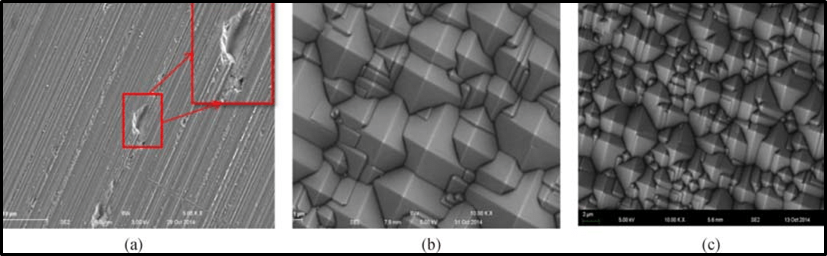
Surface of Cz-Si wafer (a) Bare Si wafer; (b) pyramid size of around 10 µm; (c) pyramid size of around 5 µm. Image source: High-quality industrial n-type silicon wafers with an efficiency of over 23% for Si heterojunction solar cells
Application of Cz-Si Wafers in Solar Cells
Solar cells are simply silicon disks which transform sunlight into electricity. These disks basically act as sources of energy in calculators, rooftop panels, telecommunications, and other smaller devices. Again, pure silicon plays a vital role in solar cells, as they form the basic element in the production process. The solar component comprises the silicon semiconductor that has a protective material around it in a metal frame. This material is equally made up of a capsule of clear silicon plastic joined around the cells, and then, put in ethylene-vinyl acetate. A glass cover is discovered on earth clothing. The electronic part on the array consists mostly of copper, while the frame is steel or aluminum.
In manufacturing a solar cell, the process begins by purifying the silicon using the floating-zone technique. Next, single crystal silicon is made, then, the silicon wafers are sliced out of the ingot. The process of doping begins, following the traditional technique or method. The next step is to put the electrical contacts in place. Then, an anti-reflecting coating is put on the wafer to lower the amount of sunlight that was lost during the process. The finished product is then sealed or encapsulated in a silicon rubber or similar material, and placed in an aluminum frame with a glass covering or plastic.

Application of Cz-Si Wafers in Aerospace
Manufacturers in the aviation sector have been using silicon wafer since its inception, owing to its excellent characteristics and properties. In the aviation industry, the silicon wafer is widely used as a binding material, coat, encapsulation of electronics, insulating and shielding sensitive tools from harsh temperatures. Its wide usage and resistance to extreme temperatures have made it an excellent and reliable choice for decades. Silicones are the major element used in the sector. It is made up of polymers which have a chemical cohesion built on a long chain of oxygen and mostly, silicon materials. Silicon wafers are very useful for aircraft OEM (Original equipment manufacturing) and also for maintenance, repair, and overhaul (MRO). Due to their frequency of use, aircraft suffer wears and damages which result in their constant replacement. Silicon wafers are a convenient choice since they are delivered in dual cartridges and tubes directly, which help to save time while avoiding waste.
Application of Cz-Si Wafers in other Electronic Appliances
Silicon wafers are widely used as semiconductors in electronic devices like transistors, integrated and printed circuits board and so on. These appliances rely on the highly conductive characteristics of silicon wafers for maximum performance. However, before silicon can function as such, the material used must be doped. The process of doping simply involves the addition of a small portion of impurity to aid the release of electrons without affecting the temperature. Two of the most commonly used silicon materials for semiconductor applications are the P and N-type materials. The P-type is made by introducing an element with atoms having one less electron than silicon itself. The effect is a + charged material. While the N-type is made by the addition of impurity to silicon with atoms having one more electron than silicon. The result is a charged material. Most electronic appliances have both silicon types in them as a reliable semiconductor for electric voltage.

Conclusion
In conclusion, it can be seen from the above discussion that the role played by Czochralski Silicon (CzSi) wafer in different industrial sectors is paramount. The material is so versatile that it can be used in numerous applications ranging from semiconductors in electronic devices to the production of solar cells, manufacture of smartphones and computers, etc. The demand for Czochralski Silicon (CzSi) wafer is drastically increasing with the passage of time.
Recent Posts
-

What is the Difference Between 7075 and 6061 Aluminum Alloy?
When comparing 7075 aluminum alloy to 6061 aluminum alloy, it's essential to understand their disti …5th Apr 2024 -

Iron-Air Batteries: The Ultimate Guide
Iron-air batteries represent a significant breakthrough in energy storage technology, offering a sus …29th Mar 2024 -

Discovering the Power of 2D Materials
In material science, the discovery of two-dimensional (2D) materials represents a transformative de …22nd Mar 2024